Electronic device including a schottky contact

a technology of schottky contacts and electronic devices, applied in the direction of semiconductor devices, diodes, electrical apparatus, etc., can solve the problems of voltage spikes within, dead time periods, and accumulation of charges

Active Publication Date: 2015-01-06
SEMICON COMPONENTS IND LLC
View PDF12 Cites 5 Cited by
  • Summary
  • Abstract
  • Description
  • Claims
  • Application Information

AI Technical Summary

Benefits of technology

[0003]When changing states of the power switching circuit, periods of dead time can occur when current cannot readily flow through the circuit, and charge accumulates in the switching devices. Once a change of state occurs, the removal of this accumulated charge can create voltage spikes within the power switching circuit that may exceed the drain-to-source breakdown voltage of one of the IGFETs. To reduce the likelihood of an over-voltage situation, a Schottky contact can be used to help reduce charge that can accumulate during a period of dead time. Dead time refers to a brief period in a switching cycle when all switching devices are off or in a non-current conducting state. Referring briefly to US 2011 / 0156682, a Schottky contact can be formed where a metal silicide structure contacts an N-type epitaxial layer. Current flows vertically from an N+ semiconductor substrate through the N-type epitaxial layer to the metal silicide structure. The power switching circuit will not have optimal performance, as compromises are made when designing such a device.

Problems solved by technology

When changing states of the power switching circuit, periods of dead time can occur when current cannot readily flow through the circuit, and charge accumulates in the switching devices.
Once a change of state occurs, the removal of this accumulated charge can create voltage spikes within the power switching circuit that may exceed the drain-to-source breakdown voltage of one of the IGFETs.
The power switching circuit will not have optimal performance, as compromises are made when designing such a device.

Method used


Image

  • Electronic device including a schottky contact
  • Electronic device including a schottky contact
  • Electronic device including a schottky contact

Examples


Embodiment Construction

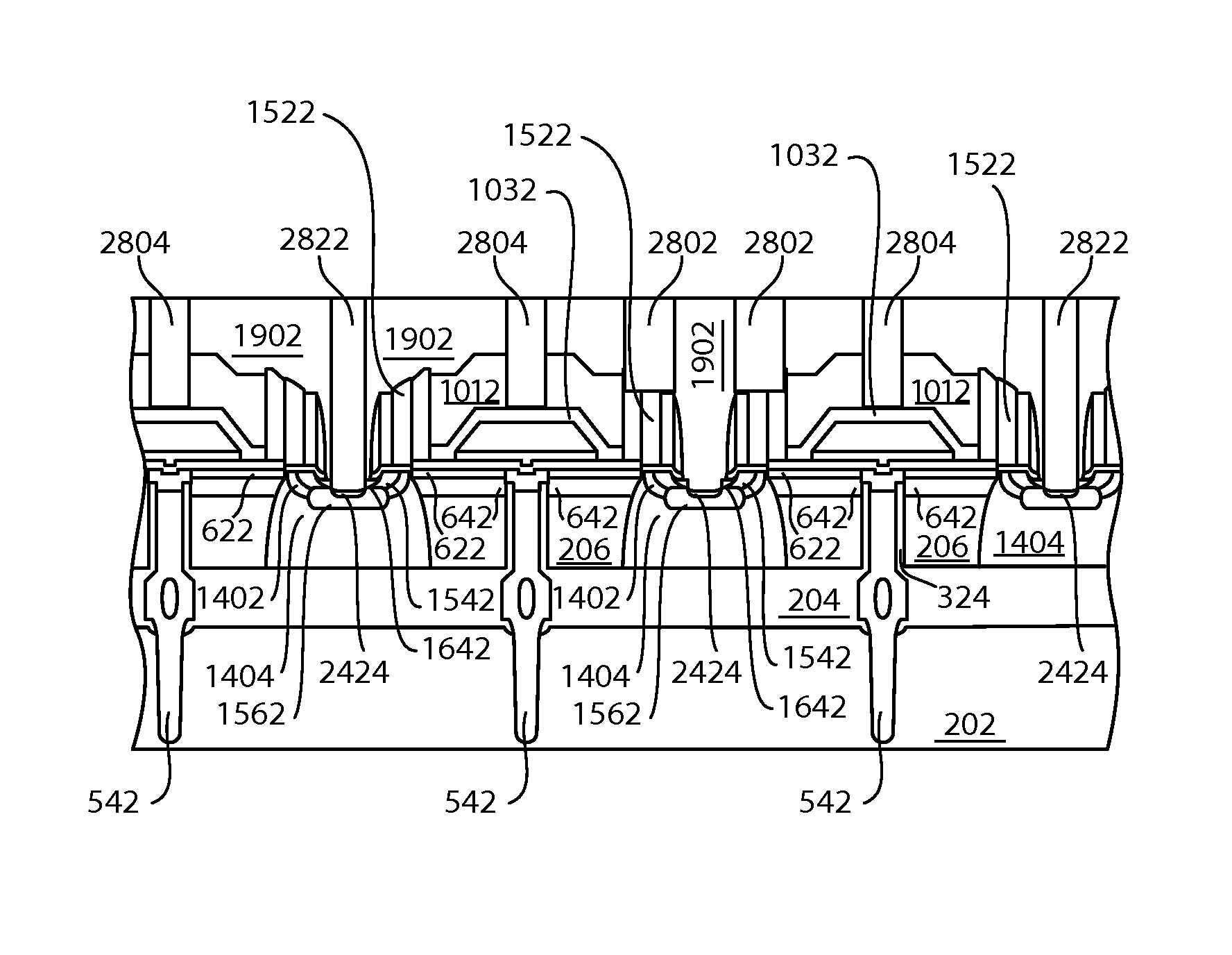
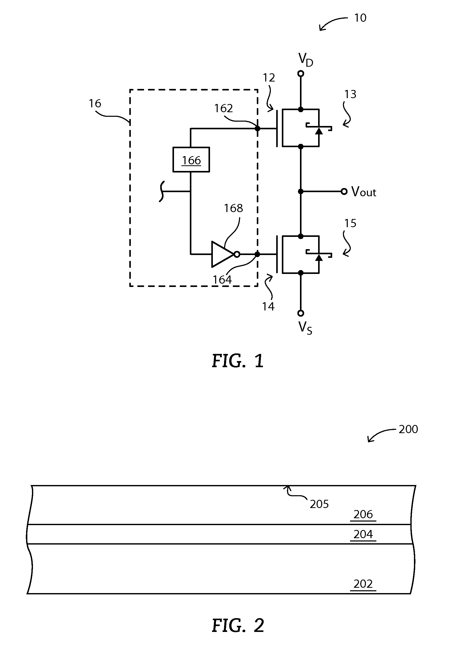
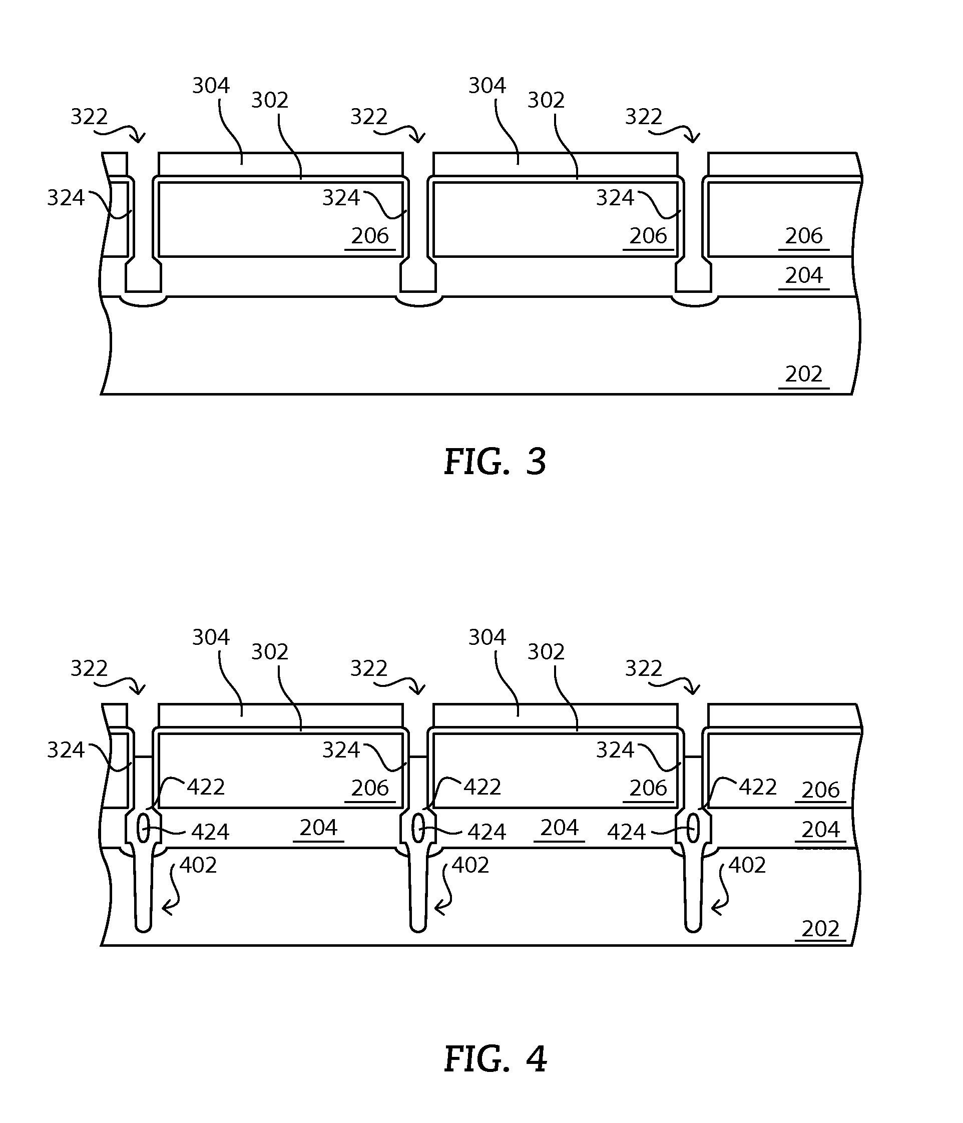
[0033]The following description in combination with the figures is provided to assist in understanding the teachings disclosed herein. The following discussion will focus on specific implementations and embodiments of the teachings. This focus is provided to assist in describing the teachings and should not be interpreted as a limitation on the scope or applicability of the teachings. However, other embodiments can be used based on the teachings as disclosed in this application.

[0034]As used herein, the terms “horizontally-oriented” and “vertically-oriented,” with respect to a region or structure, refer to the principal direction in which current flows through such region or structure. More specifically, current can flow through a region or structure in a vertical direction, a horizontal direction, or a combination of vertical and horizontal directions. If current flows through a region or structure in a vertical direction or in a combination of directions, wherein the vertical comp...


PUM


Abstract

An electronic device can include a semiconductor layer having a primary surface, and a Schottky contact comprising a metal-containing member in contact with a horizontally-oriented lightly doped region within the semiconductor layer and lying adjacent to the primary surface. In an embodiment, the metal-containing member lies within a recess in the semiconductor layer and contacts the horizontally-oriented lightly doped region along a sidewall of the recess. In other embodiment, the Schottky contact may not be formed within a recess, and a doped region may be formed within the semiconductor layer under the horizontally-oriented lightly doped region and have a conductivity type opposite the horizontally-oriented lightly doped region. The Schottky contacts can be used in conjunction with power transistors in a switching circuit, such as a high-frequency voltage regulator.

Description

FIELD OF THE DISCLOSURE[0001]The present disclosure relates to electronic devices and processes of forming electronic devices, and more particularly to, electronic devices including Schottky contacts and processes of forming the same.RELATED ART[0002]An insulated gate field-effect transistor (IGFET) is a common type of transistor that can be used in a power switching circuit. An IGFET includes a source region, a drain region, a channel region extending between the source and drain regions, and a gate structure provided adjacent to the channel region. The gate structure includes a gate electrode layer disposed adjacent to and separated from the channel region by a thin dielectric layer.[0003]When changing states of the power switching circuit, periods of dead time can occur when current cannot readily flow through the circuit, and charge accumulates in the switching devices. Once a change of state occurs, the removal of this accumulated charge can create voltage spikes within the pow...

Claims


Application Information

Patent Timeline
Patent Type & Authority Patents(United States)
IPC IPC(8): H01L29/76H01L27/02
CPCH01L27/0255H01L29/063H01L29/1095H01L29/4175H01L29/7816H01L29/7824H01L29/872
Inventor LOECHELT, GARY H.VENKATRAMAN, PRASADHOSSAIN, ZIAGRIVNA, GORDON M.
Owner SEMICON COMPONENTS IND LLC
Why Eureka
Try Eureka