Leadframe package with dual lead configurations

a leadframe and configuration technology, applied in the field of semiconductor package technology, can solve the problems of parasitic capacitance, degrade the signal delivery and overall performance characteristics of the semiconductor chip, and the loc package also exhibits certain limitations, so as to improve the intrinsic function and performance of the various leads, improve the performance of the resulting leadframe package, and reduce noise

Inactive Publication Date: 2007-02-22
SAMSUNG ELECTRONICS CO LTD
View PDF8 Cites 15 Cited by
  • Summary
  • Abstract
  • Description
  • Claims
  • Application Information

AI Technical Summary

Benefits of technology

[0013] The detailed description provided below discloses combinations of lead frames, bonding wires and bonding pad configurations useful for manufacturing LOC semiconductor device packages in which various lead configurations are utilized for leads dedicated to different functions for improving the intrinsic function and performance of the various leads. Example embodiments of the invention include leadframe packages in which combinations of signal leads exhibiting improved signal delivery characteristics and / or fixed voltage leads exhibiting reduced noise improve the performance of the resulting leadframe packages. Leadframe packages incorporating the lead configurations according to the example embodiments of the invention will tend to exhibit improved high-speed performance.

Problems solved by technology

LOC packages also tend to exhibit certain limitations, particularly when used with higher speed devices, that have contributed to the increasing use of BGA packages.
In particular, the construction of an LOC package in which elongated leads are disposed above an active surface of a semiconductor chip results in parasitic capacitance.
Increasing levels of parasitic capacitance, induced between the signal leads and the active surface of the semiconductor chip in an LOC package, tends to degrade the signal delivery and overall performance characteristics of the semiconductor chip.
With regard to the fixed voltage leads provided in an LOC package, e.g., power and ground leads, the noise tends to increase as a result of the inductance effects associated with high speed operation of a semiconductor chip.
Additionally, all of the signal leads 120 illustrated in FIG. 1A are structured as single layer delivery lines which will also tend to degrade the high speed performance of such signal leads.
Accordingly, as the speed of the semiconductor chip increases, noise, attributed to, for example, simultaneous switching noise (SSN) increases and the power delivery characteristics deteriorate.

Method used


Image

  • Leadframe package with dual lead configurations
  • Leadframe package with dual lead configurations
  • Leadframe package with dual lead configurations

Examples


first example embodiment

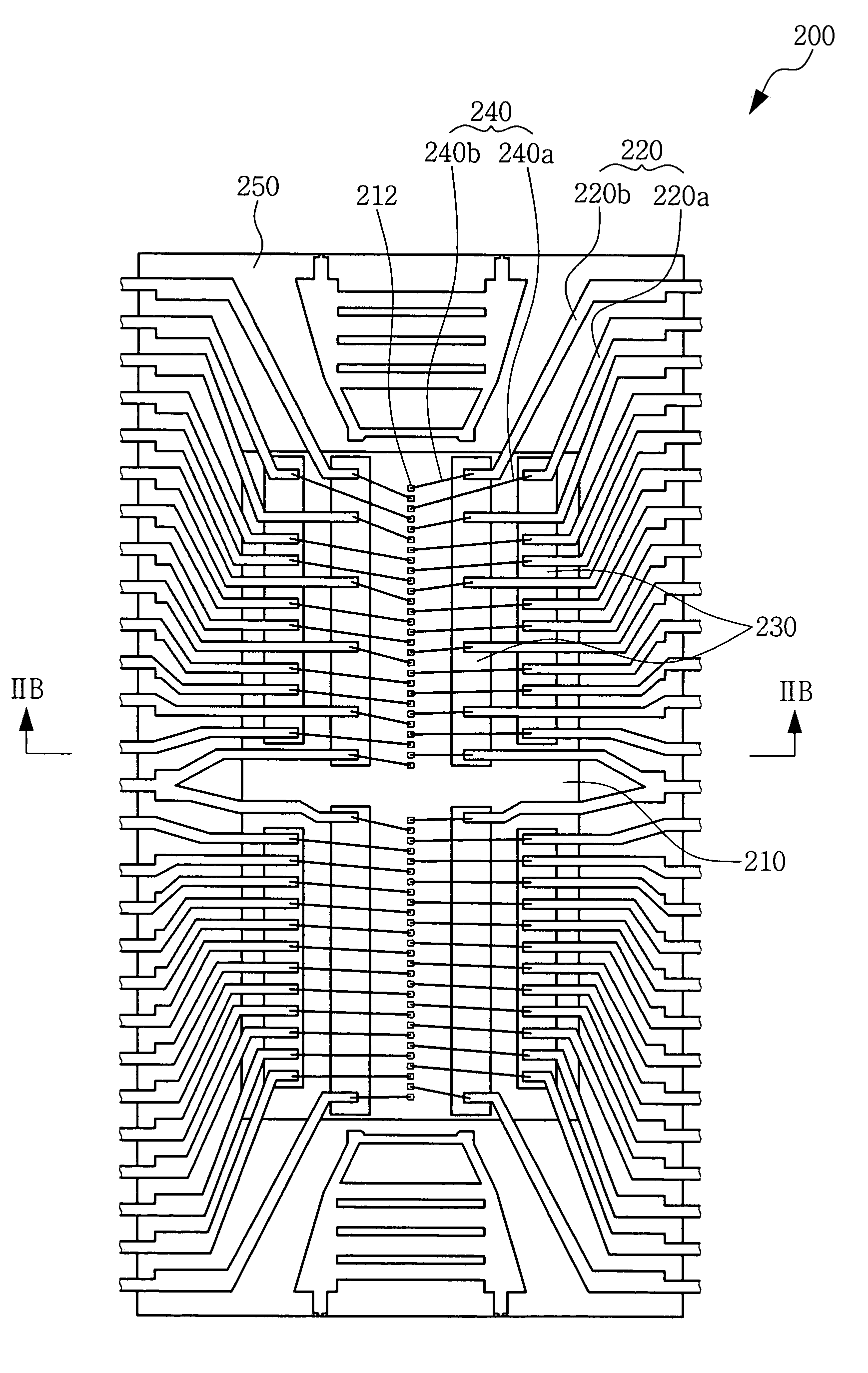
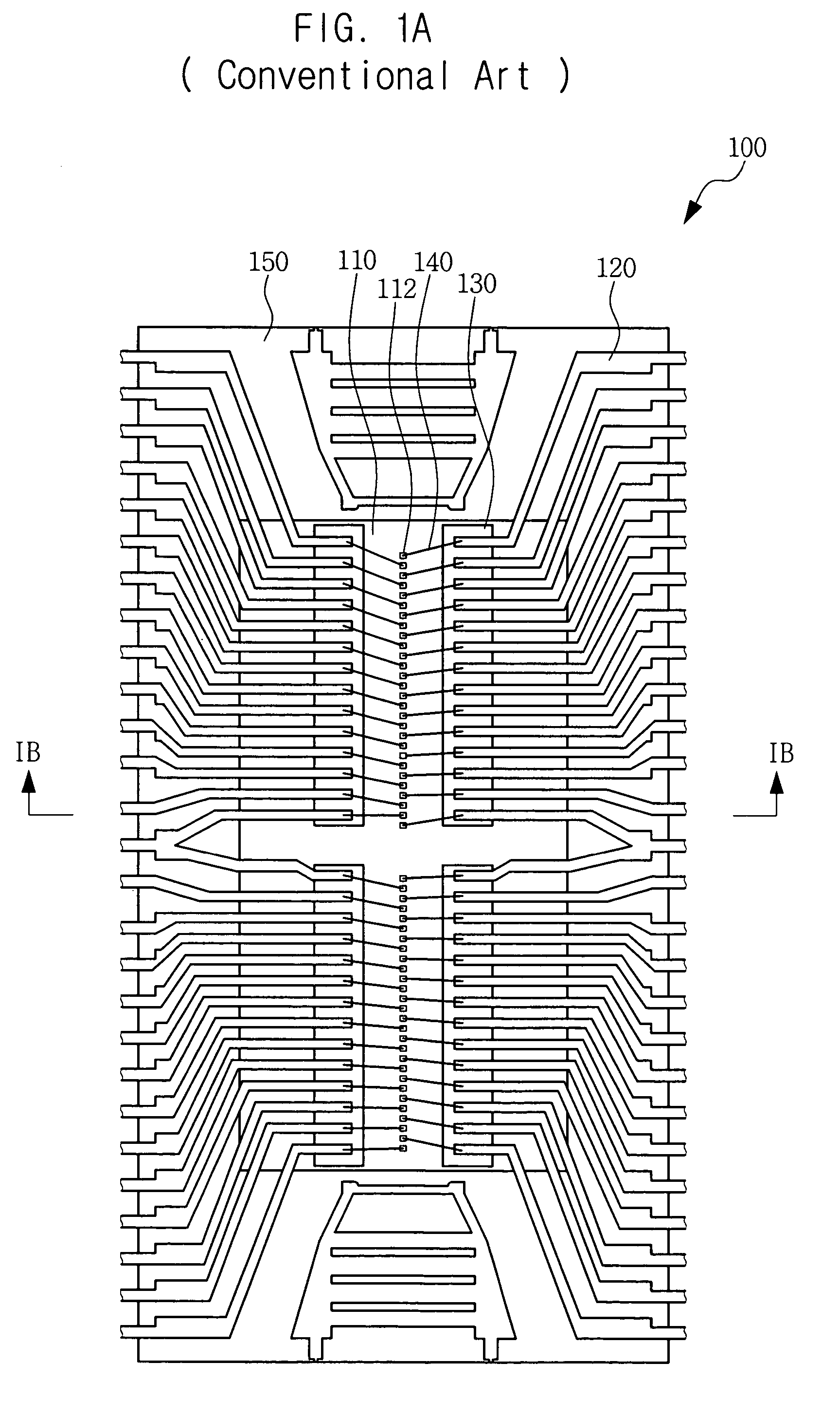
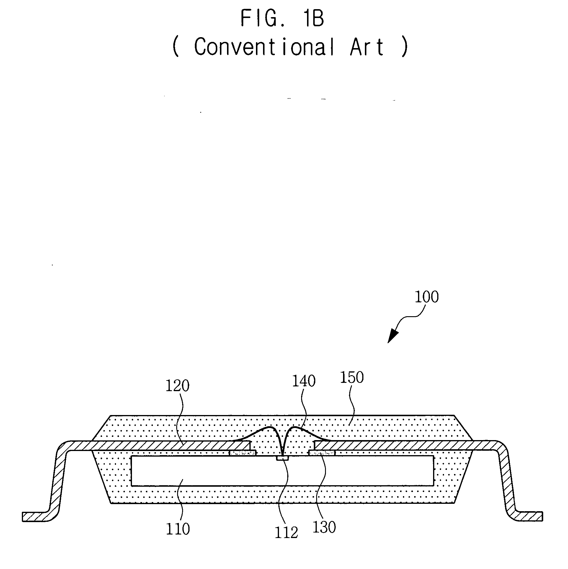
[0034]FIG. 2A is a plan view of a leadframe package 200 according to a first example embodiment of the present invention. FIG. 2B is a cross-sectional view of FIG. 2A taken along the line IIB-IIB (that is, cut along a plane running through the length of a lead 220). As illustrated in FIGS. 2A and 2B, the package 200 according to a first example embodiment is an LOC type package with leads 220 extending over portions of the active surface of semiconductor chip 210. In this example embodiment, the leads 220 are attached to the active surface of the semiconductor chip by strips or regions of adhesive 230, for example, adhesive tape.

[0035] A plurality of chip pads 212 are aligned in a single row generally along a central longitudinal axis of the active surface of the semiconductor chip 210, with leads 220 generally disposed on either side of the axis and extending across the active surface of the semiconductor chip and towards the chip pads 212. Each of the chip pads 212 is individuall...

second example embodiment

[0044]FIGS. 3A and 3B illustrate, respectively, a plan view and cross-sectional view of a leadframe package 300 according to a second example embodiment of the present invention. FIG. 3A illustrates a portion of the package 300 extending from an axis adjacent and parallel to the central longitudinal axis along which chip pads 212 are aligned along the active surface of the semiconductor chip and the outer periphery of the semiconductor chip 210. FIG. 3B illustrates a cross-sectional view taken along a plane extending along the length direction of a lead 320 as generally suggested in FIG. 2B. One or more regions of adhesive tape as described above in connection with FIG. 2A according to a first example embodiment of the invention are omitted from FIG. 3A in the interest of clarity and to reduce the complexity of the drawing but are reflected in FIG. 3B as element 230.

[0045] As illustrated in FIGS. 3A and 3B, the package 300 according to a second example embodiment has a characterist...

third example embodiment

[0058] Illustrated in FIGS. 5A and 5B are a plan view and cross-sectional view of a leadframe package 500 according to a third example embodiment of the invention with FIG. 5B representing a cross-sectional view taken along a plane extending in the length direction along a lead 220 as in FIGS. 2B and 3B.

[0059] As illustrated in FIGS. 5A and 5B, the package 500 according to a third example embodiment includes chip pads 512 that are not all centrally located on the active surface of the semiconductor chip 210. To the extent that the components and / or features of the example embodiments of the leadframe packages 200, 300 and / or 400 illustrated in, for example, FIGS. 2A, 2B, 3A, 3B and 4 and described above are similar or identical to those found in leadframe package 500, identical reference numerals will be used and the detailed explanation of these components and / or features will be omitted.

[0060] The chip pads 512 included in this third example embodiment are configured in three se...


PUM


Abstract

The invention provides a variety of leadframe packages in which signal connections and fixed voltage connections are configured differently to improve the relative performance of the connections relative to their assigned function. The signal connections incorporate one or more configurations of signal lead and corresponding signal bonding wires that tend to reduce the relative capacitance of the signal connectors and thereby improve high speed performance. The fixed voltage connections incorporate configurations of fixed voltage leads and fixed voltage bonding wires that will tend to reduce the inductance of the fixed voltage connector and reduce noise on the fixed voltage connections and improve power delivery characteristics. The configurations of the associated signal and fixed voltage connections will tend to result in signal connections that include signal leads that are shorter, narrower and / or more widely separated from the active surface of the semiconductor chip than the corresponding fixed voltage leads.

Description

PRIORITY STATEMENT [0001] This U.S. non-provisional application claims priority under 35 U.S.C.§ 119 from Korean Patent Application No. 2005-76996, which was filed on Aug. 22, 2005, the contents of which are incorporated herein, in its entirety, by reference, and is a continuation-in-part of U.S. patent application Ser. No. 11 / 261,569, filed Oct. 31, 2005, which claims priority under 35 U.S.C. § 119 from Korean Patent Application No. 2004-92447, which was filed on Nov. 12, 2004, the contents of both of which are incorporated herein, in their entirety, by reference.BACKGROUND OF THE INVENTION [0002] 1. Field of the Invention [0003] The present invention relates to a semiconductor package technology and, more particularly, to leadframe packages having dual lead configurations in which the signal leads and the fixed voltage leads are configured differently. [0004] 2. Description of the Related Art [0005] A leadframe packages having a lead-on-chip (LOC) type configuration have been used...

Claims


Application Information

Patent Timeline
Patent Type & Authority Applications(United States)
IPC IPC(8): H01L23/495
CPCH01L23/4951H01L23/49513H01L24/06H01L2224/04042H01L2224/06136H01L2224/32245H01L2224/48091H01L2224/48247H01L2224/4826H01L2224/49171H01L2224/4943H01L2224/73215H01L2224/92247H01L2924/01005H01L2924/01082H01L2924/078H01L2924/30105H01L2924/30107H01L2924/00014H01L24/32H01L24/48H01L24/49H01L2924/01006H01L2924/01033H01L2924/00H01L2224/73265H01L2224/49109H01L2924/00012H01L2224/05554H01L2924/181H01L2224/45015H01L2924/207H01L2224/45099H01L23/495
Inventor LEE, JONG-JOOAHN, MEE-HYUN
Owner SAMSUNG ELECTRONICS CO LTD
Why Eureka
Try Eureka