Semiconductor device, spread spectrum clock generator and method thereof

a spread spectrum clock and electromagnetic clock technology, applied in the direction of electrical equipment, angle demodulation by phase difference detection, automatic control, etc., can solve the problems of electromagnetic waves, limited shielding devices, and harm to the human body

Active Publication Date: 2007-02-22
SAMSUNG ELECTRONICS CO LTD
View PDF7 Cites 42 Cited by
  • Summary
  • Abstract
  • Description
  • Claims
  • Application Information

AI Technical Summary

Problems solved by technology

The harmonic component included in higher-frequency clock signals may cause electromagnetic waves which, in some cases, may be harmful to the human body.
Conventionally, a shielding device (e.g., a capacitor) may be used to reduce the electromagnetic waves generated by the system, but such shielding devices may be limited with respect to a degree to which they may reduce the electromagnetic waves.
However, in general, a number of signals output from the VCO 240 may be relatively limited.
Accordingly, if more than three signals having different phases are output from the VCO 240, it may be difficult or impossible to obtain a maximum possible frequency modulation ratio of 0.5% using the above-described conventional process.

Method used


Image

  • Semiconductor device, spread spectrum clock generator and method thereof
  • Semiconductor device, spread spectrum clock generator and method thereof
  • Semiconductor device, spread spectrum clock generator and method thereof

Examples


Embodiment Construction

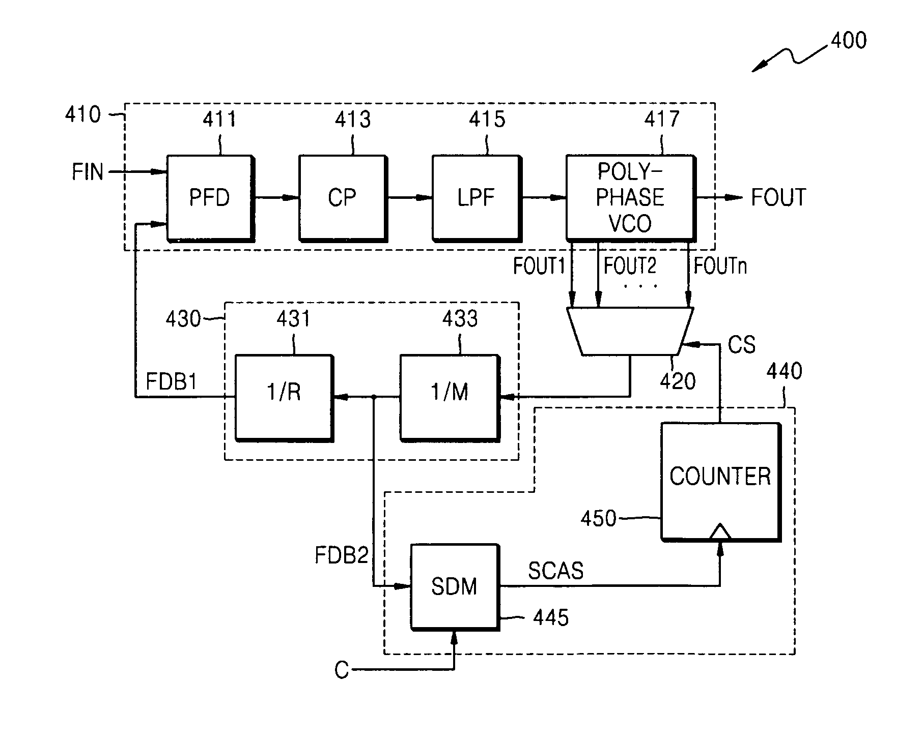
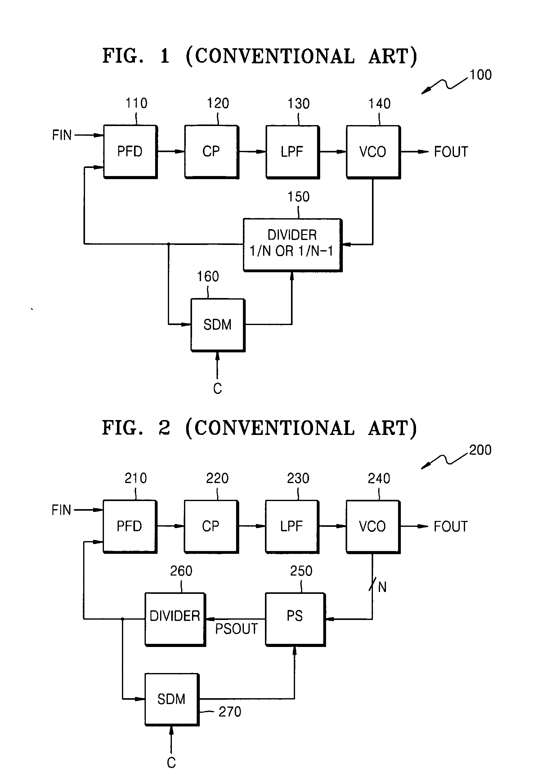
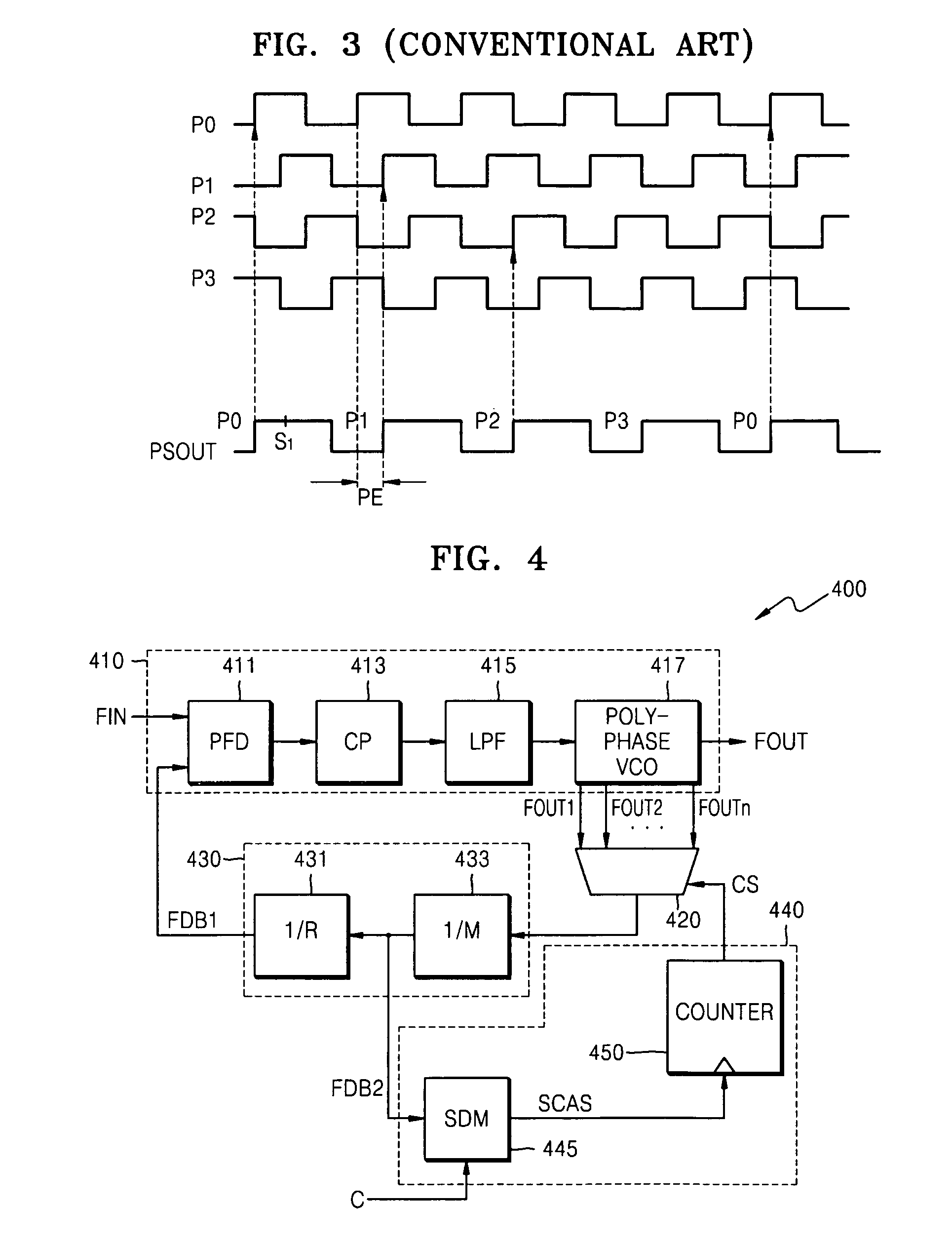
[0033] Example embodiments of the present invention are described more fully hereinafter with reference to the accompanying drawings, in which example embodiments of the present invention are shown. Example embodiments of the present invention may, however, be embodied in many different forms and should not be construed as limited to the example embodiments set forth herein. Rather, these example embodiments are provided so that this disclosure will be thorough and complete, and will fully convey the scope of the invention to those skilled in the art. Like numbers refer to like elements throughout.

[0034] It will be understood that although the terms first and second are used herein to describe elements and should not be limited by these terms. These terms are used to distinguish one element from another. Thus, a first element discussed below could be termed a second region, layer or section, and similarly, a second element may be termed a first element without departing from the te...


PUM


Abstract

A semiconductor device, a spread spectrum clock generator and method thereof are provided. The example semiconductor device may include a frequency dividing unit receiving an output signal, generating a first feedback signal and a second feedback signal by dividing a frequency of the received output signal, and a phase offset unit outputting the output signal having a predetermined or desired phase difference with a reference signal in response to the second feedback signal, wherein the second feedback signal having a higher frequency than the first feedback signal. The example spread spectrum clock generator may include a plurality of frequency dividers which are connected in series and a selector selecting and outputting one of a plurality of output signals, each of the plurality of output signals having a different phase difference with respect to a reference signal, in response to at least one output from one or more of the plurality of frequency dividers. The example method may include receiving a reference signal with a first frequency, generating a feedback signal having a second frequency, the second frequency higher than the first frequency and outputting at least one of a sequentially selected set of output signals in response to the generated feedback signal.

Description

PRIORITY STATEMENT [0001] This application claims the priority of Korean Patent Application No. 10-2005-0075674, filed on Aug. 18, 2005, in the Korean Intellectual Property Office, the disclosure of which is incorporated herein in its entirety by reference. BACKGROUND OF THE INVENTION [0002] 1. Field of the Invention [0003] Example embodiments of the present invention relate generally to a semiconductor device, a spread spectrum clock generator and method thereof and more particularly to a semiconductor device, a spread spectrum clock generator and method of outputting signals. [0004] 2. Description of the Related Art [0005] Increases in the operating speed of systems may cause an increase the speed at which data may be processed. Generally, to increase a data processing speed, a clock signal frequency may be increased. However, higher-frequency clock signals may contain a harmonic component. The harmonic component included in higher-frequency clock signals may cause electromagnetic...

Claims


Application Information

Patent Timeline
Patent Type & Authority Applications(United States)
IPC IPC(8): H03D3/24
CPCH03L7/081H03L7/0891H03L7/0996H03L7/18H03L7/08
Inventor SHIN, JONG-SHIN
Owner SAMSUNG ELECTRONICS CO LTD
Why Eureka
Try Eureka