Manufacturing method of solid-state imaging device and solid-state imaging device

a solid-state imaging and manufacturing method technology, applied in the direction of semiconductor devices, electrical equipment, basic electric elements, etc., can solve the problems of deteriorating image quality, reducing the area of photodetecting portions, and reducing the amount of charge each pixel can handle, so as to prevent inter-pixel bloom

Inactive Publication Date: 2007-02-22
FUJIFILM CORP
View PDF1 Cites 20 Cited by
  • Summary
  • Abstract
  • Description
  • Claims
  • Application Information

AI Technical Summary

Benefits of technology

The patent text describes a method to prevent inter-pixel bloking while ensuring necessary areas for photodetecting portions are secured without increasing the voltage required for the process. This results in improved image quality and reduced noise in the image sensor.

Problems solved by technology

The technical problem addressed in this patent text is how to prevent inter-pixel bloming in a solid-state imaging device without increasing the sweep-into-substrate voltage and reducing the area of the photodetecting portions, while also preventing charge leakage between pixels in a deep place in the substrate.

Method used


Image

  • Manufacturing method of solid-state imaging device and solid-state imaging device
  • Manufacturing method of solid-state imaging device and solid-state imaging device
  • Manufacturing method of solid-state imaging device and solid-state imaging device

Examples


first embodiment

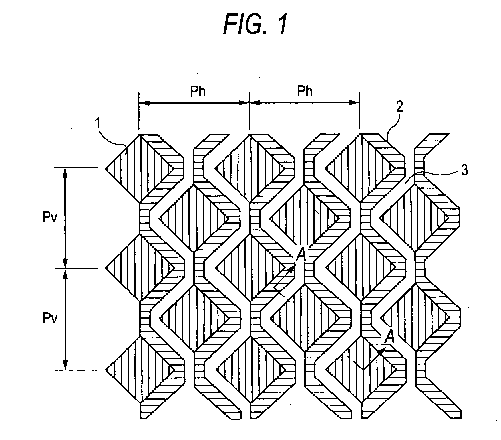
[0052]FIG. 1 is a schematic plan view showing the structure of a substrate surface in an exemplary solid-state imaging device according to the invention.

[0053] As shown in FIG. 1, a large number of photodiodes (photodetecting portions, pixel portions) 1 are arranged on the surface of a semiconductor substrate in plural columns and plural rows at constant pitches Ph and Pv. FIG. 1 is a simplified view, and in an actual device hundreds to thousands of photodiodes 1 are arranged in each column or row. Each photodiode 1 stores charge of an amount corresponding to a quantity of light received.

[0054] The photodiodes 1 belonging to the even-numbered columns are deviated from those belonging to the odd-numbered columns by about ½of the pitch Pv of the photodiodes 1 of each column, and the photodiodes 1 belonging to the even-numbered rows are deviated from those belonging to the odd-numbered rows by about ½of the pitch Ph of the photodiodes 1 of each row. A staggered pixel arrangement (hon...

second embodiment

[0108] Next, a second embodiment of the invention will be described with reference to FIGS. 10-12.

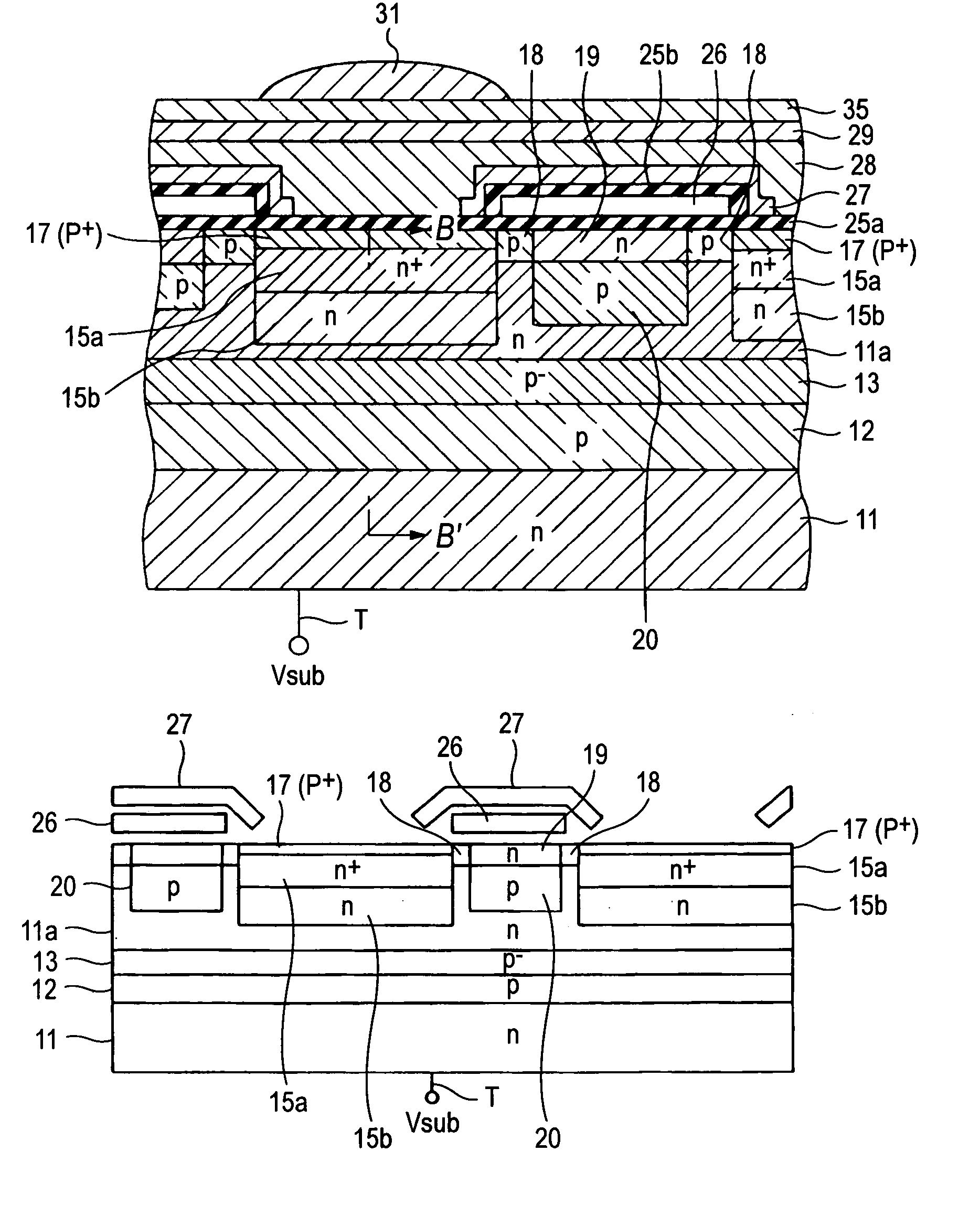
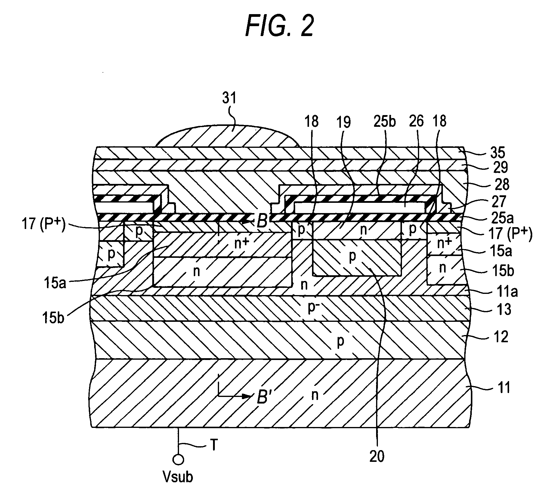
[0109]FIG. 10 is a sectional view showing the structure of an important part of a solid-state imaging device manufactured by a manufacturing method according to the second embodiment of the invention (an epitaxial layer is laid on an n-type epitaxial substrate and plural inter-pixel isolation regions are formed in multiple layers).

[0110]FIG. 10 corresponds to FIG. 3, and regions etc. having corresponding ones in FIG. 3 are given the same reference symbols as the latter. The structure of the solid-state imaging device shown in FIG. 10 is characterized in that an epitaxial layer 40 is laid on an n-type epitaxial substrate (i.e., the portion under a broken line in FIG. 10 and a margin in the depth direction is thereby increased (to secure sufficient sensitivity to long-wavelength light), and that plural impurity regions (20, 30, and 32) arranged in multiple layers serve as inter-pixel is...


PUM


Abstract

A manufacturing method of a solid-state imaging device, the device comprising: a semiconductor substrate; photodiodes each comprising a surface-side first conductivity type region formed adjacent to a surface of the semiconductor substrate and a second conductivity type region provided directly under the surface-side first conductivity type region; a second conductivity type vertical transfer region provided in the vicinity of the surface-side first conductivity type region; at least one first conductivity type inter-pixel isolation region provided under the vertical transfer region; and at least one first conductivity type overflow barrier region provided below the first conductivity type inter-pixel isolation region, the method comprising: a first step of forming the first conductivity type overflow barrier region in a semiconductor substrate; and a second step of ion-implanting first conductivity type impurity ions from a direction in which channeling tends to occur, to form at least one of the first conductivity type inter-pixel isolation region.

Description


Claims


Application Information

Patent Timeline
Owner FUJIFILM CORP
Why Eureka
Try Eureka