Manufacturing method of a semiconductor device

a manufacturing method and semiconductor technology, applied in semiconductor devices, semiconductor/solid-state device details, electrical devices, etc., can solve the problems of difficult to realize both a high activation ratio, poor controllability of hole injection from a collector electrode, and high production cost of igbt using the double epitaxial wafer, etc. corrosion of the contact electrode can be prevented, high breakdown voltage, excellent switching characteristics

Active Publication Date: 2008-03-27
RENESAS ELECTRONICS CORP
View PDF8 Cites 31 Cited by
  • Summary
  • Abstract
  • Description
  • Claims
  • Application Information

AI Technical Summary

Benefits of technology

[0017]An IGBT having high breakdown voltage and excellent switching characteristics can be realized by using a semiconductor substrate made of FZ single crystal silicon, and carrying out activation annealing of a field stop layer and activation annealing of a collector region, respectively to attain activation ratios of impurity ions suited for the field stop layer and co

Problems solved by technology

However, the production cost of the IGBT using the double epitaxial wafer is high because it uses double epitaxial crystals more expensive than FZ crystals.
It also has a further problem such as poor controllability of hole injection from a collector electrode due to variations in the concentration of the collector region.
In this IGBT, however, activation annealing for n type impurity ions and that for p type impurity ions are carried out simulta

Method used


Image

  • Manufacturing method of a semiconductor device
  • Manufacturing method of a semiconductor device
  • Manufacturing method of a semiconductor device

Examples


embodiment 1

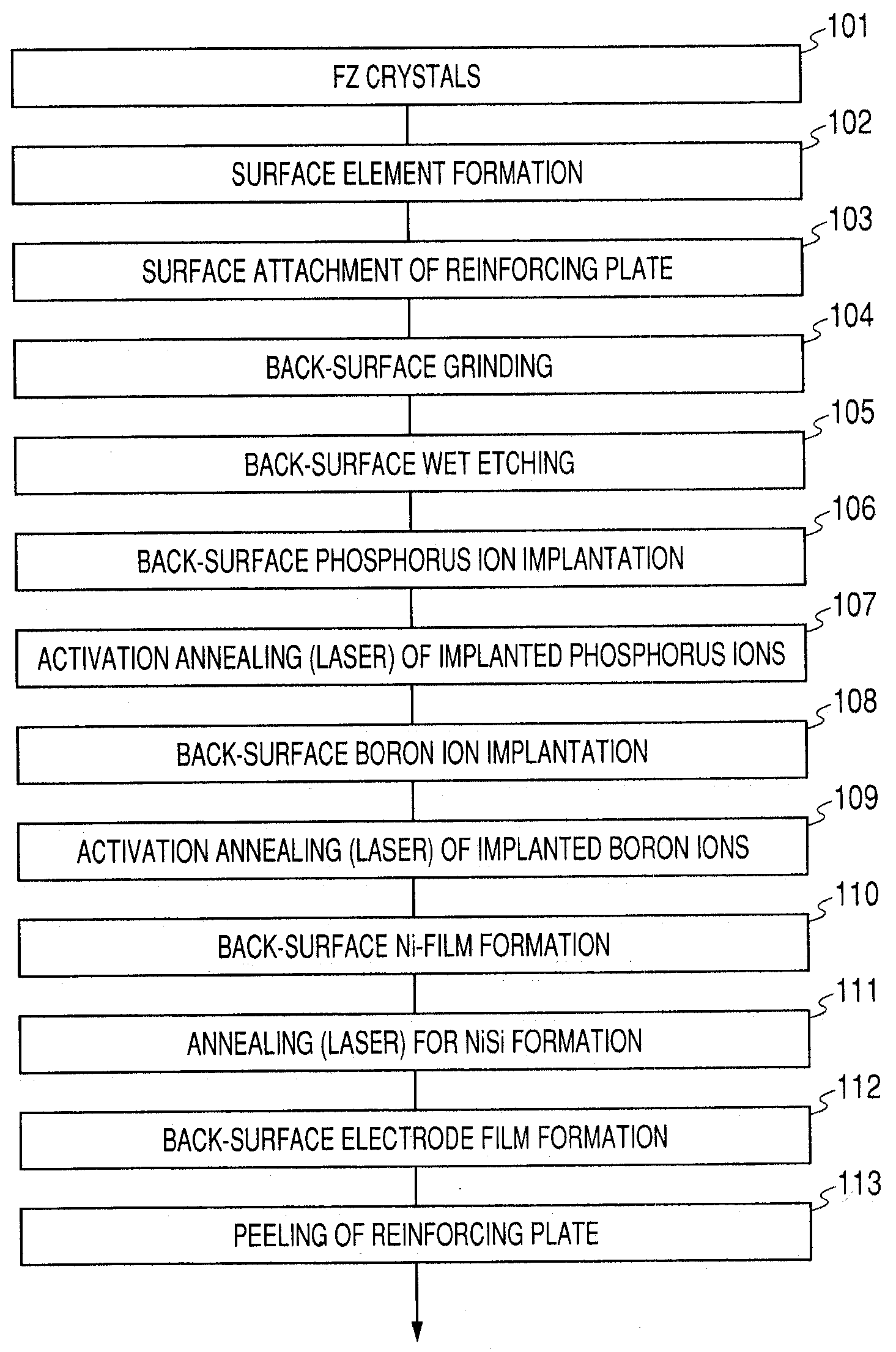
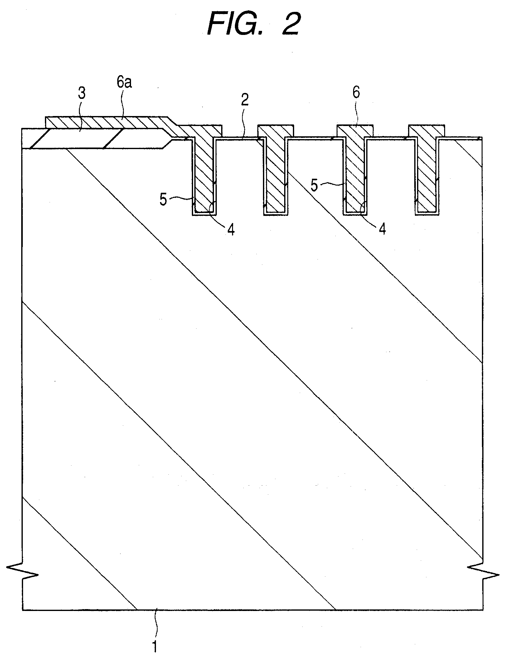
[0042]A semiconductor device according to Embodiment 1 has an IGBT with an LiPT (Low Injection Punch Through) structure as a semiconductor element. The semiconductor device according to this Embodiment 1 will next be described in accordance with the manufacturing steps based on FIGS. 1 to 16. FIG. 1 is a flow chart of the manufacturing method of the semiconductor device; FIGS. 2 to 8 are fragmentary cross-sectional views illustrating the manufacturing method of the semiconductor device; FIG. 9 is a graph showing displaced silicon atoms generated by the implantation of boron ions; FIG. 10 is a graph showing the relationship between the switch-off time (tf) and activation ratio of boron ions of the IGBT; FIG. 11 is a graph showing the relationship between the on-voltage (Vce) and switch-off time (Tf) of the IGBT; and FIGS. 12 to 16 are fragmentary cross-sectional views illustrating the manufacturing method of the semiconductor device.

[0043]As illustrated in FIG. 2, a semiconductor sub...

embodiment 2

[0079]A semiconductor device according to Embodiment 2 has, similar to the above-described one according to Embodiment 1, an IBGT having an LiPT structure as a semiconductor element, but is different from it in the thickness of the semiconductor substrate. In Embodiment 1, described was an IGBT using a semiconductor substrate having a thickness not greater than 120 μm (for example, from 70 to 120 μm). In Embodiment 2, on the other hand, an IGBT uses a semiconductor substrate having a thickness exceeding 120 μm and the reinforcing plate used in Embodiment 1 is not used during the fabrication of the IGBT. Such a semiconductor device of Embodiment 2 will be described based on FIGS. 17 to 21. FIG. 17 is a flow chart of the manufacturing method of the semiconductor device; and FIGS. 18 to 21 are fragmentary cross-sectional views illustrating the manufacturing method of the semiconductor device. Manufacturing steps until the formation of an emitter electrode (interconnect 15) of the IGBT ...


PUM


Abstract

Provided is a technology of carrying out activation annealing of n type impurity ions implanted for the formation of a field stop layer (n+ type semiconductor region) and activation annealing of p type impurity ions implanted for the formation of a collector region (p+ type semiconductor region) in separate steps to adjust an activation ratio of the n type impurity ions in the field stop layer to 60% or greater and an activation ratio of the p type impurity ions in the collector region to from 1 to 15%. This makes it possible to form an IGBT having a high breakdown voltage and high-speed switching characteristics. Moreover, use of a film stack made of nickel silicide, titanium, nickel and gold films for a collector electrode makes it possible to provide an ohmic contact with the collector region.

Description

CROSS-REFERENCE TO RELATED APPLICATIONS[0001]The disclosure of Japanese Patent Application No. 2006-262732 filed on Sep. 27, 2006 including the specification, drawings and abstract is incorporated herein by reference in its entirety.BACKGROUND OF THE INVENTION[0002]The present invention relates to a manufacturing technology of a semiconductor device, particularly to a technology effective when applied to the manufacture of an insulated gate bipolar transistor (which will hereinafter be abbreviated as IGBT).[0003]In Japanese Patent Laid-Open No. 2003-59856 (Paragraph [0012], FIG. 5), there is described a technology which includes implanting impurity ions into the back surface of an FZ wafer and carrying out heat treatment for activating the implanted ions by using laser annealing with pulse laser having a wavelength of from 240 to 1070 nm and a half bandwidth of from 100 to 500 nm or using, in combination, this laser annealing and low-temperature furnace annealing.[0004]In Japanese P...

Claims


Application Information

Patent Timeline
IPC IPC(8): H01L21/265
CPCH01L23/49562H01L29/41766H01L29/42356H01L29/66348H01L29/7397H01L2224/32245H01L2224/45144H01L2224/73265H01L2224/48247H01L2924/13055H01L2924/1305H01L2924/00
Inventor MIYASHITA, ISAOFUJII, YUJIEBARA, HAJIMEISHIZAKA, KATSUOHOSOYA, NORIOOKUDA, HIDEKAZU
Owner RENESAS ELECTRONICS CORP
Why Eureka
Try Eureka