Semiconductor device having reduced effective substrate resistivity and associated methods

a technology of resistivity and effective substrate, applied in the field of semiconductor devices, can solve the problems of increased power dissipation required for the chip, undesired contact resistance, and high resistance, and achieve the effect of reducing the effective substrate resistivity and reducing the specific resistan

Inactive Publication Date: 2007-02-22
FAIRCHILD SEMICON CORP
View PDF16 Cites 14 Cited by
  • Summary
  • Abstract
  • Description
  • Claims
  • Application Information

AI Technical Summary

Benefits of technology

[0008] In view of the foregoing background, it is therefore an object of the present invention to provide a semiconductor device and associated

Problems solved by technology

A higher on-resistance translates into greater power dissipation required for the chip.
Unfortunately, the on-resistance contribution from the unscalable regions of the integrated circuit, such as the substrate, for example, remain constant even as cell densities are increased.
The relatively high resistivity of conventional substrates may also cause undesired contact resist

Method used


Image

  • Semiconductor device having reduced effective substrate resistivity and associated methods
  • Semiconductor device having reduced effective substrate resistivity and associated methods
  • Semiconductor device having reduced effective substrate resistivity and associated methods

Examples


Embodiment Construction

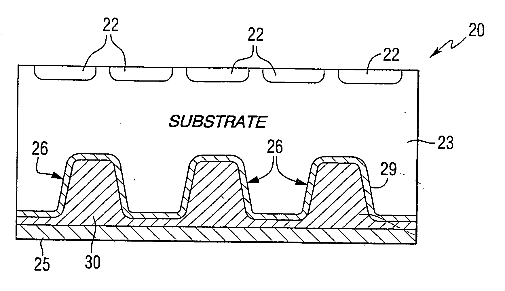
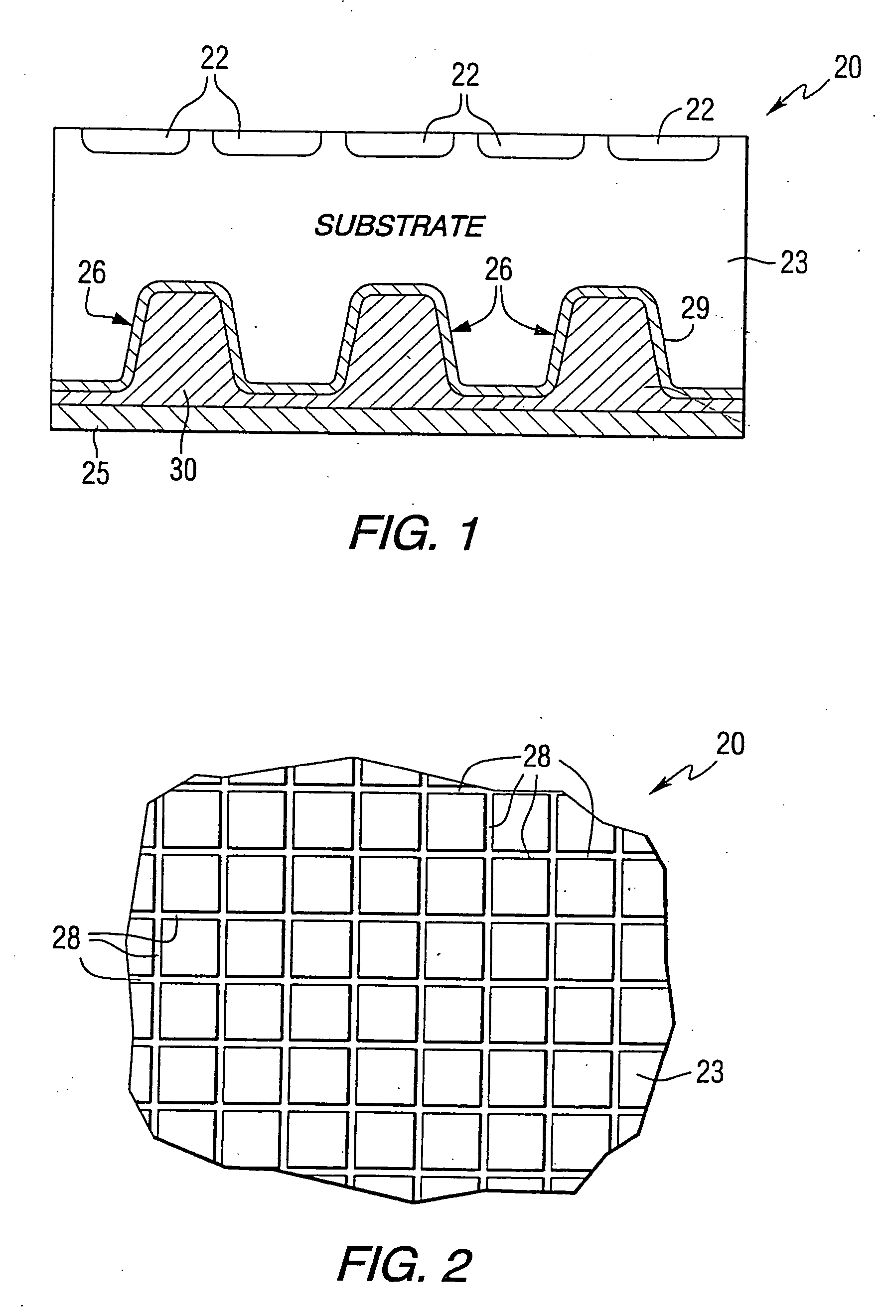
[0032] The present invention will now be described more fully hereinafter with reference to the accompanying drawings, in which preferred embodiments of the invention are shown. This invention may, however, be embodied in many different forms and should not be construed as limited to the embodiments set forth herein. Rather, these embodiments are provided so that this disclosure will be thorough and complete, and will fully convey the scope of the invention to those skilled in the art. Like numbers refer to like elements throughout, and the thicknesses of certain layers may be exaggerated in the drawings for clarity.

[0033] Referring initially to FIGS. 1 and 2 an embodiment of a semiconductor device 20 having a lowered effective substrate resistivity is described. The lowered effective substrate resistivity results in a lowered specific on-resistance, for example, when the invention is is implemented in a power MOSFET device, for example, as will be readily appreciated by those skil...


PUM


Abstract

A semiconductor device includes at least one device active region formed in a first surface of a semiconductor substrate, an electrical contact layer on a second surface of the semiconductor substrate, and at least one resistivity-lowering body positioned in a corresponding recess in the substrate and connected to the electrical contact layer. The body preferably comprises a material having an electrical resistivity lower than an electrical resistivity of the semiconductor substrate to thereby lower an effective electrical resistivity of the substrate. The device active region may be an active region of a power control device, such as a MOSFET or IGBT, for example. The body may preferably comprise an electrical conductor such as copper, aluminum, silver, solder, or doped polysilicon. The at least one recess and associated resistivity-lower body preferably defines a proportion of the semiconductor substrate area adjacent the device active region greater than about 0.4 percent, and may extend into the semiconductor substrate a distance greater than about 25 percent of a thickness of the substrate.

Description

FIELD OF THE INVENTION [0001] The present invention relates to semiconductors, and, more particularly, to a semiconductor device, such as a power MOSFET having reduced on-resistance. BACKGROUND OF THE INVENTION [0002] Semiconductor devices, typically in the form of integrated circuits, are widely used in almost all electronic equipment, such as handheld calculators, personal computers, automobiles, cellular telephones, and sophisticated mainframe computers. A typical semiconductor device includes a semiconductor substrate which, in turn, includes a number of active devices formed adjacent a first surface of the substrate. For example, one or more power metal-oxide semiconductor field-effect transistors (MOSFETs) may be formed in active regions of the substrate. Power MOSFETs are often used because of their relatively high switching speeds as compared to bipolar transistors, for example. Power MOSFETs may be used in power conversion or motor control circuitry. [0003] The so-called “o...

Claims


Application Information

Patent Timeline
IPC IPC(8): H01L21/336
CPCH01L29/0657H01L29/41741H01L29/41766H01L29/456H01L29/7395H01L29/0873H01L2924/01013H01L2924/01029H01L2924/14H01L2924/13091H01L29/7802
Inventor ZENG, JUN
Owner FAIRCHILD SEMICON CORP
Why Eureka
Try Eureka