System and method for cutting liquid crystal display substrate

a technology of liquid crystal display and system, applied in the direction of manufacturing tools, instruments, transportation and packaging, etc., can solve the problems of long cutting process and unresolved above-described problems, and achieve the effect of fast cutting system

Inactive Publication Date: 2007-03-01
SAMSUNG ELECTRONICS CO LTD
View PDF5 Cites 18 Cited by
  • Summary
  • Abstract
  • Description
  • Claims
  • Application Information

AI Technical Summary

Benefits of technology

[0005] The present invention provides a faster cutting system for a liquid crystal display (LCD) substrate in which a first cutting unit cuts the LCD substrate in one direction into a plurality of sub-substrates each including at least one panel, a carrier unit separates the sub-substrates from each other and simultaneously carries the separated sub-substrates.

Problems solved by technology

In a conventional second cutting system, only a single sub-substrate is cut at one time to prevent cross cutting, and therefore, the cutting process takes a long time.
Various cutting methods including one disclosed in Korea Patent Publication No. 2003-086727, entitled “Scribe / Break System for Cutting LCD Substrate” have been proposed, but the above-described problem has not be solved.

Method used


Image

  • System and method for cutting liquid crystal display substrate
  • System and method for cutting liquid crystal display substrate
  • System and method for cutting liquid crystal display substrate

Examples


first embodiment

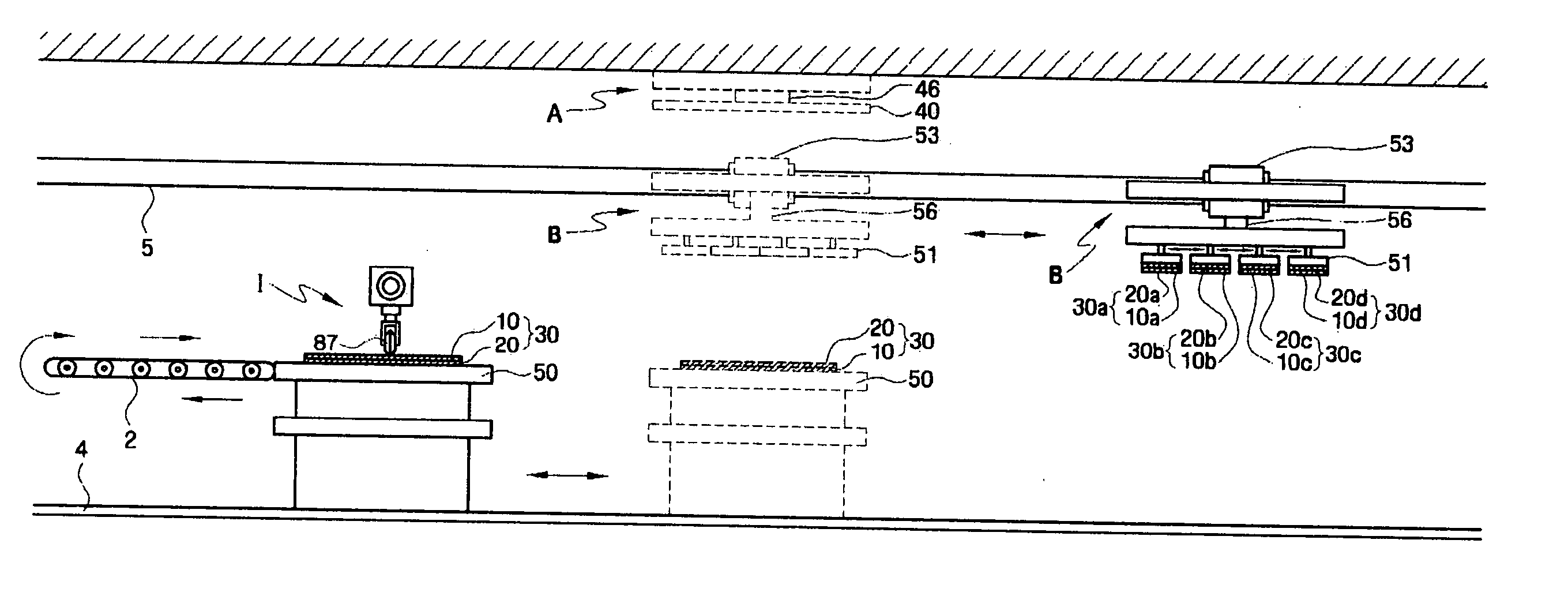
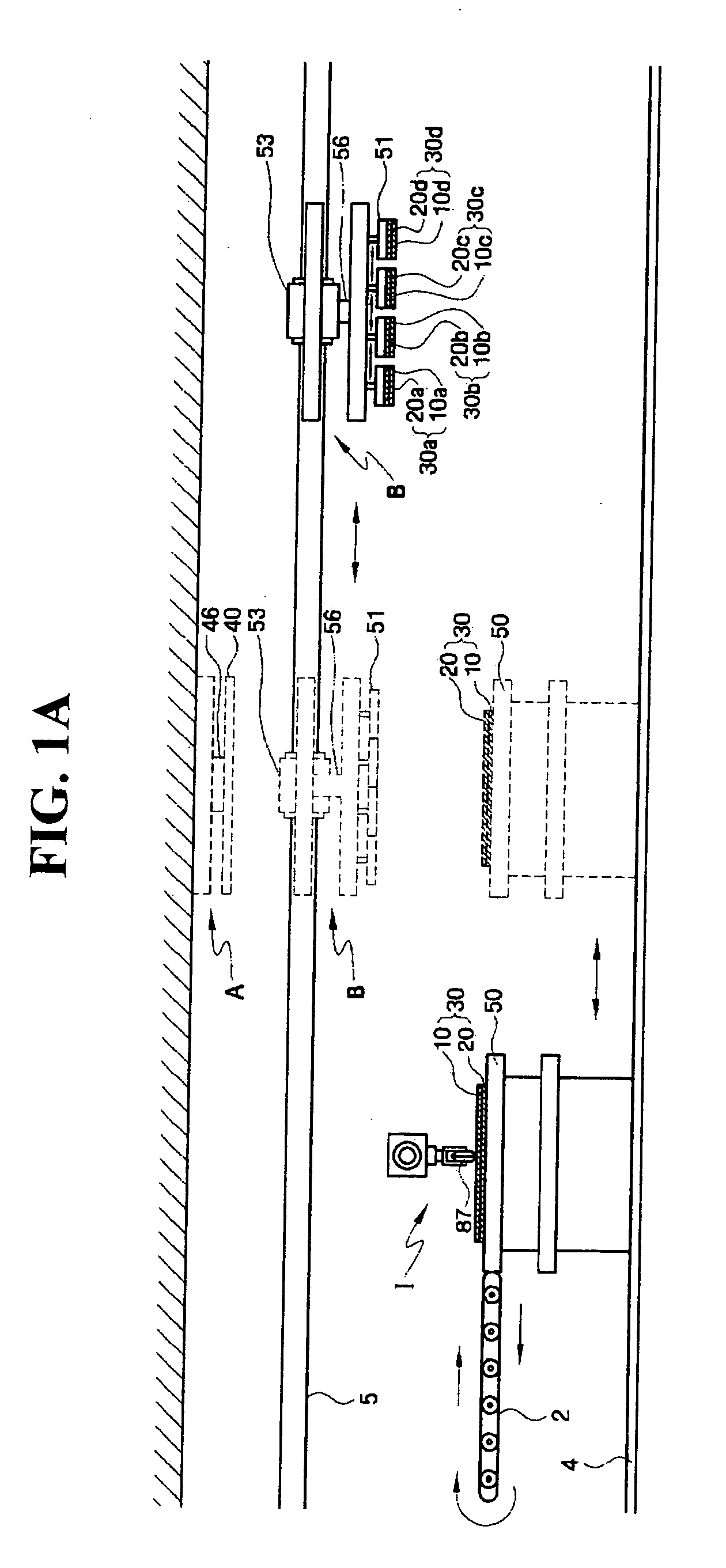
[0029] The method of cutting the substrate 30 using the cutting system having the above-described structure will be described with reference to FIGS. 1A through 5H. FIGS. 5A through 5H illustrate stages in a cutting process performed by the cutting system according to the present invention. The substrate 30 carried by the first carrier 2 is placed onto the first mount 50 in a shape shown in FIG. 5A. After the substrate 30 is placed onto the first mount 50, the first mount 50 moves toward the first cutting portion ‘I’. Thereafter, one side 10 of the substrate 30 on the first mount 50 is cut in the longitudinal direction by the first cutting portion ‘I’, as shown in FIG. 5B. In detail, the wheel 87 of the first cutting portion ‘I’ moves along the central axle 82 so that the one side 10 of the substrate 30 is cut forming a cutting line 11 in FIG. 5B. Then, the first mount 50 proceeds by a width of a sub-substrate. Thereafter, the wheel 87 moves along the central axle 82 so that the one...

second embodiment

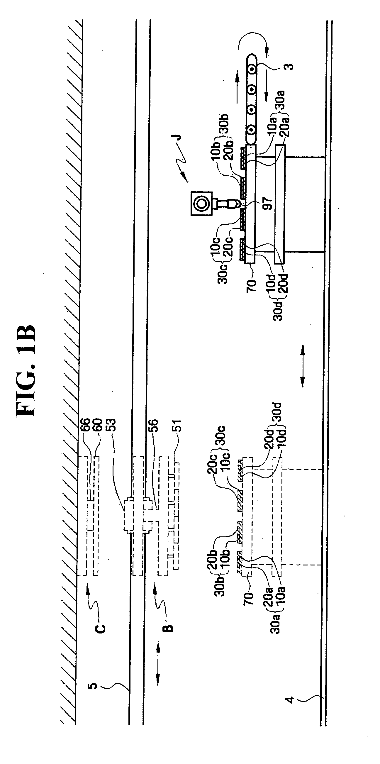
[0049] In addition, the cutting system according to the present invention may include a reversing unit D. The reversing unit D reverses the substrate 30 whose one side has been cut in the longitudinal direction by the first cutting portion ‘I’ and the sub-substrates 30a, 30b, 30c, and 30d whose one sides have been cut in the transverse direction by the second cutting portion ‘J’. For this operation, the reversing unit D includes a reversing unit suction plate 510, a reversing unit cylinder 560, and a reversing unit rotator 530.

[0050] The reversing unit cylinder 560 lifts up and down the reversing unit suction plate 510 so that the reversing unit suction plate 510 can suck and hold the substrate 30 and the sub-substrates 30a, 30b, 30c, and 30d. The one side 10 of the substrate 30 placed on the first mount 50 and the sides 20a, 20b, 20c, and 20d of the respective sub-substrates 30a, 30b, 30c, and 30d placed on the second mount 70 are sucked by the reversing unit suction plate 510. For...


PUM

PropertyMeasurementUnit
distanceaaaaaaaaaa
hardnessaaaaaaaaaa
electricalaaaaaaaaaa

Abstract

A cutting system and method for a liquid crystal display (LCD) substrate in which a first cutting unit cuts the LCD substrate in one direction into a plurality of sub-substrates each including at least one panel, a carrier unit separates the sub-substrates from each other and simultaneously carries the separated sub-substrates to a second cutting unit that cuts the separated sub-substrates into individual LCDs.

Description

REFERENCE TO RELATED APPLICATION [0001] This application claims priority from Korean Patent Application No. 10-2005-0078345 filed on Aug. 25, 2005 in the Korean Intellectual Property Office, the disclosure of which is incorporated herein by reference in its entirety. FIELD OF THE INVENTION [0002] The present invention relates to a system for cutting a liquid crystal display (LCD) substrate, and more particularly, to a faster cutting system DESCRIPTION OF THE RELATED ART [0003] An LCD displays image information by using the electrical and optical characteristics of liquid crystals injected between two sheets of material. LCDs consume less power and are lighter and smaller than cathode ray tubes. Accordingly, LCDs are widely used in a display of portable computers, monitors of desktop computers, and monitors for high-definition video system, etc. Manufacturing LCDs includes forming a first display plate and a second display plate each having at least one unit panel, a process of bondi...

Claims


Application Information

Patent Timeline
Patent Type & Authority Applications(United States)
IPC IPC(8): B26D1/00
CPCB28D5/0011B65G49/066B65G2249/045C03B33/03C03B33/07G02F1/133351Y10T83/04Y02P40/57G02F1/13
Inventor KANG, HO-MINCHOI, WEON-WOOBOK, SEUNG-LYONG
Owner SAMSUNG ELECTRONICS CO LTD
Why Eureka
Try Eureka