Memory device and manufacturing method thereof

Inactive Publication Date: 2007-03-01
MACRONIX INT CO LTD
View PDF7 Cites 1 Cited by
  • Summary
  • Abstract
  • Description
  • Claims
  • Application Information

AI Technical Summary

Benefits of technology

[0009] Accordingly, the present invention is directed to a memory device and a manufacturing method thereof to improve the operational speed of the memory device.
[0010] The present invention is also directed to a memory device and a manufacturing method thereof to enhance the reliability of the memory device.
[0029] Because the substrate material of the present invention has a forbidden gap larger than that of silicon, the energy barrier between the substrate and the first insulation layer of the present invention is smaller. When the memory device is programmed or erased, electrons or holes can be easily injected into the charge storage layer from the substrate, or into the substrate from the charge storage layer. Accordingly, the operational speed of the memory device can be improved.
[0030] Further, as the substrate material of the present invention has a forbidden gap larger than that of silicon, the anode hot hole impact effect to the first insulation layer, i.e., the tunneling dielectric layer, can be reduced, while the FN tunneling method is applied to the memory device. The reliability of the memory device is thus enhanced.

Problems solved by technology

If a channel hot electron injection (CHEI) method is used, the small forbidden gap of silicon creates a large energy barrier between the silicon substrate and a tunneling dielectric layer.
As a result, the operational efficiency of the memory device declines.
It also results in the anode hot hole impact effect and damages the tunneling dielectric layer.

Method used


Image

  • Memory device and manufacturing method thereof
  • Memory device and manufacturing method thereof
  • Memory device and manufacturing method thereof

Examples


Embodiment Construction

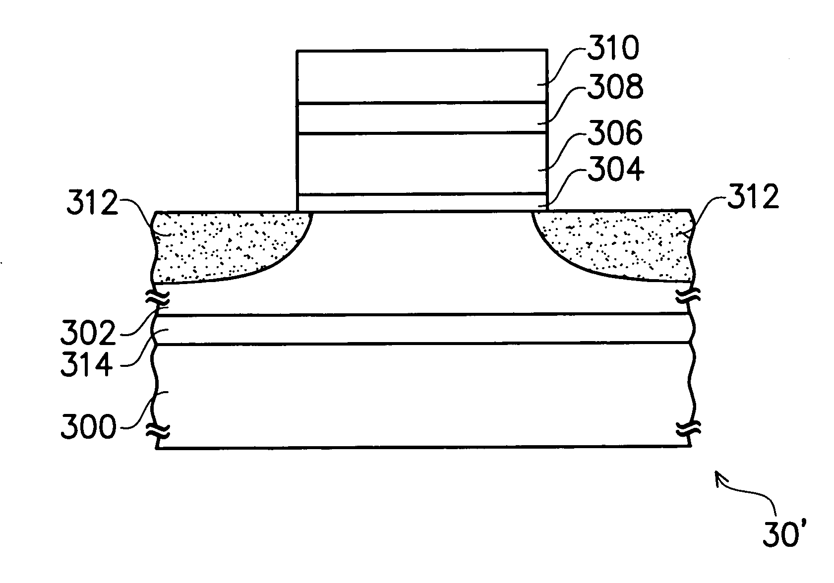
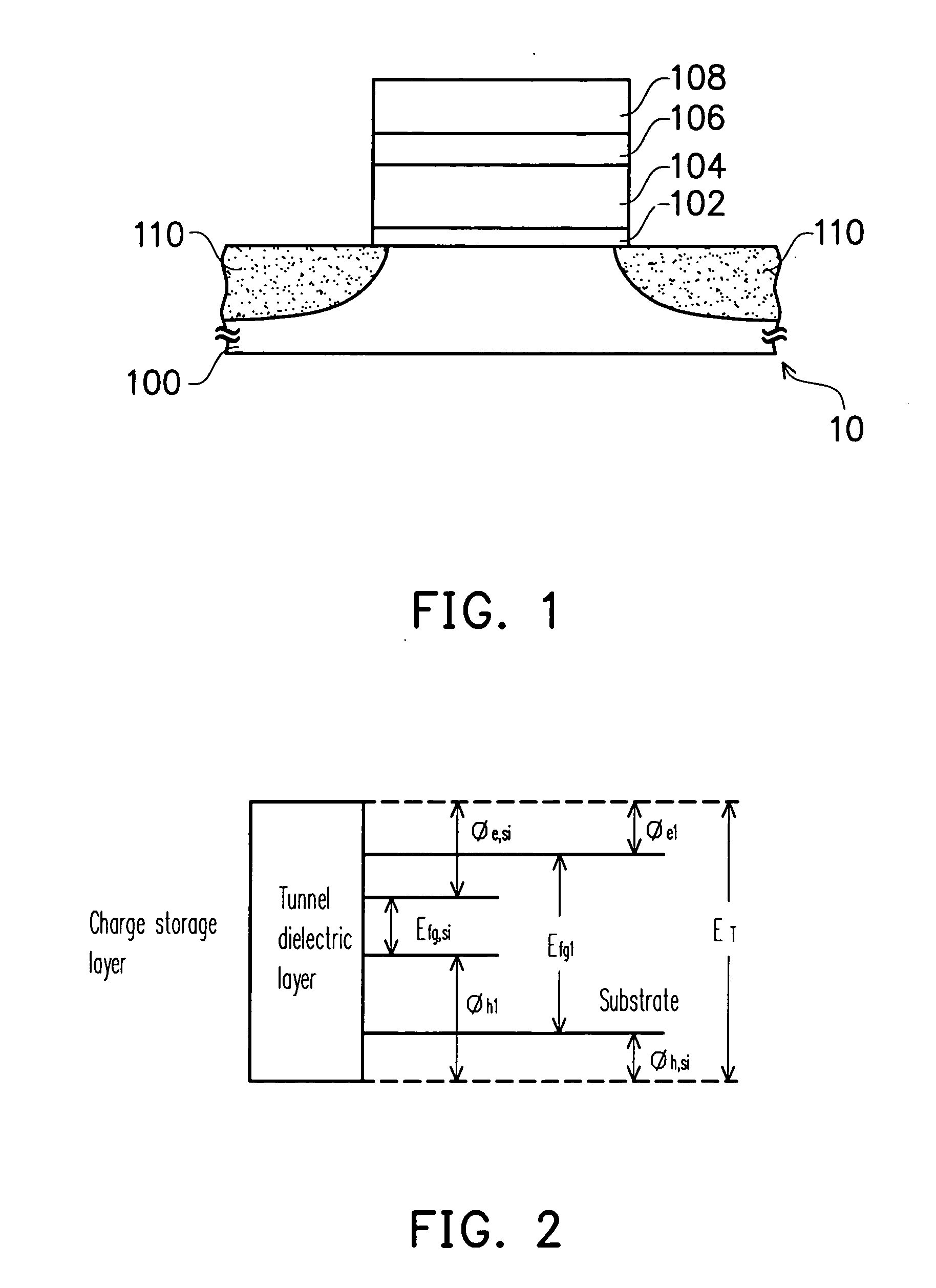
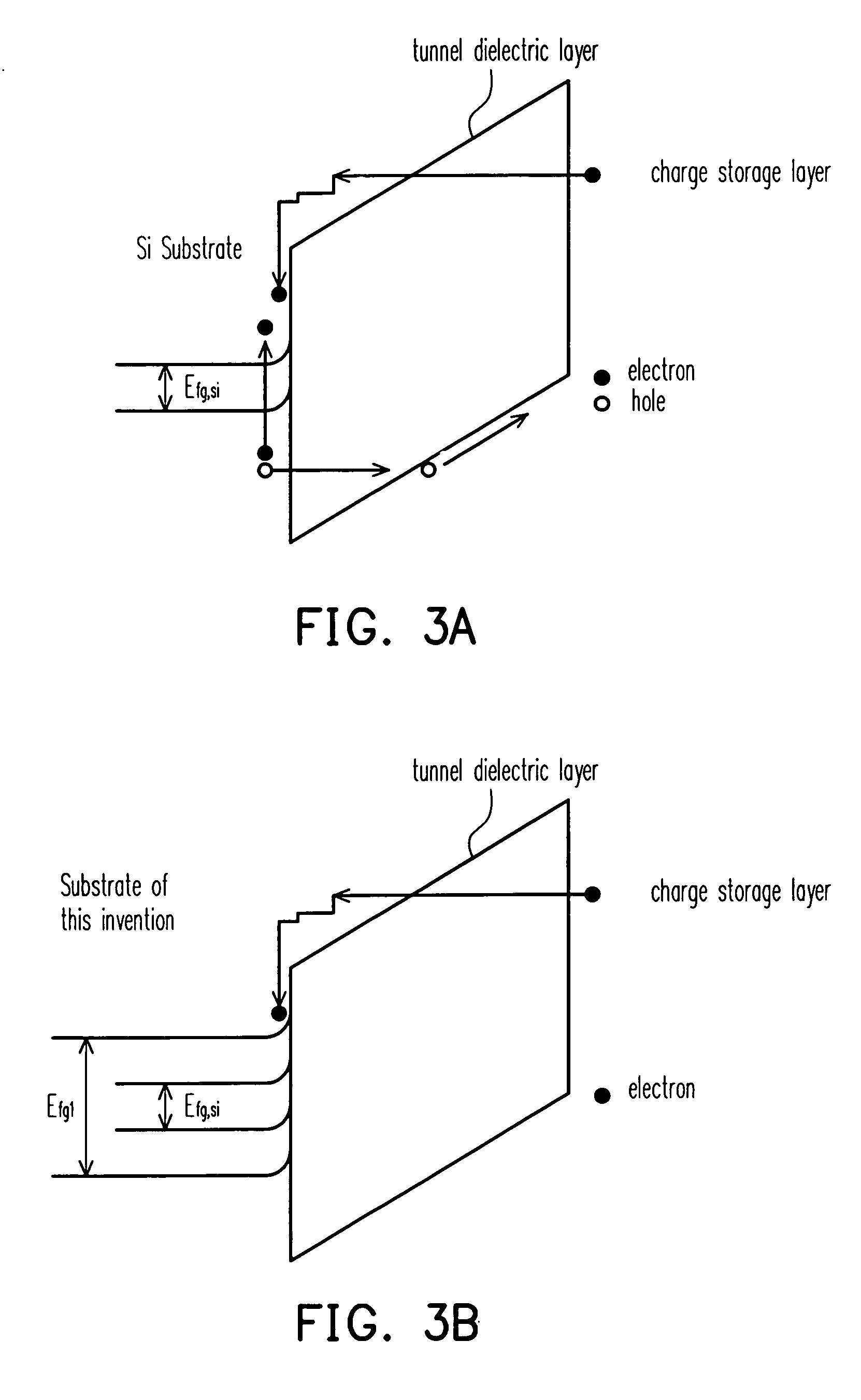
[0040]FIG. 1 is a schematic cross sectional view of a memory device according to a preferred embodiment of the present invention. Referring to FIG. 1, the memory device 10 of this embodiment comprises a substrate 100, an insulation layer 102, a charge storage layer 104, an insulation layer 106, a gate electrode layer 108, and source / drain regions 110. In this embodiment, the insulation layer 102 is disposed over the substrate 100. The charge storage layer 104 is disposed over the insulation layer 102. The insulation layer 106 is disposed over the charge storage layer 104. The gate electrode layer 108 is disposed over the insulation layer 106. Wherein, the gate electrode layer 108, the insulation layer 106, the charge storage layer 104, and the insulation layer 102 constitute a stacked structure. The source / drain regions 110 are disposed in the substrate 100 adjacent to two sides of the stacked structure. Note that the forbidden gap of the substrate 100 is larger than that of silicon...


PUM


Abstract

A memory device comprising a substrate, a first insulation layer, a charge storage layer, a second insulation layer, a gate electrode layer and source / drain regions is provided. The forbidden gap of the substrate is larger than the forbidden gap of silicon. The first insulation layer is disposed over the substrate. The charge storage layer is disposed over the first insulation layer. The second insulation layer is disposed over the charge storage layer. The gate electrode layer is disposed over the second insulation layer. The gate electrode layer, the second insulation layer, the charge storage layer and the first insulation layer constitute a stacked structure. The source / drain regions are disposed in the substrate adjacent to two sides of the stacked structure.

Description

BACKGROUND OF THE INVENTION [0001] 1. Field of the Invention [0002] The present invention relates to a semiconductor device and a manufacturing method thereof, and more particularly, to a memory device and a manufacturing method thereof. [0003] 2. Description of the Related Art [0004] Lately, since functions of computer micro-processors have been improved day by day, amount of data operated and calculated by software is also increased. As a result, expectations for memory devices are in a way higher and higher. In order to fabricate memory devices with high capacities and low costs so as to meet these requirements, it is now the semiconductor manufacturers' aim to produce memory devices with highly integrated density. [0005] Volatile and non-volatile memory devices such as erasable-and-programmable read-only memories (EPROMs), electrically-erasable-programmable read-only memories (E2PROMs), flash memories, and DRAMs can at many times read, write or erase data stored therein. Accordi...

Claims


Application Information

Patent Timeline
IPC IPC(8): H01L29/76
CPCH01L21/28273H01L29/792H01L29/7881H01L29/1608H01L29/40114
Inventor WANG, SZU-YU
Owner MACRONIX INT CO LTD
Why Eureka
Try Eureka