Semiconductor device and semiconductor chip

a semiconductor chip and semiconductor technology, applied in semiconductor devices, semiconductor/solid-state device details, electrical equipment, etc., can solve problems such as affecting inspection efficiency, reducing the area of mounting surfaces, and affecting reliability of electrical connections

Inactive Publication Date: 2007-03-01
SEIKO EPSON CORP
View PDF18 Cites 9 Cited by
  • Summary
  • Abstract
  • Description
  • Claims
  • Application Information

AI Technical Summary

Benefits of technology

[0020] The invention may provide a semiconductor device and a semiconductor chip having a metal electrode (bump) which is provided on a small electrode pad and may improve mounting capability and inspection efficiency.
[0009] a metal electrode provided at least in the opening and including a first portion provided vertically above at least part of the electrode pad and a second portion, an area of a top surface of the second portion being larger than an area of a top surface of the first portion.

Problems solved by technology

A decrease in the area of the mounting surface may impair reliable electrical connection with the interconnect pattern of the substrate.
Moreover, when inspecting the electrical characteristics of the semiconductor chip using the bump, inspection efficiency may be decreased due to the small contact surface with an inspection terminal.

Method used


Image

  • Semiconductor device and semiconductor chip
  • Semiconductor device and semiconductor chip
  • Semiconductor device and semiconductor chip

Examples


first embodiment

[0052] 1.1. First Embodiment

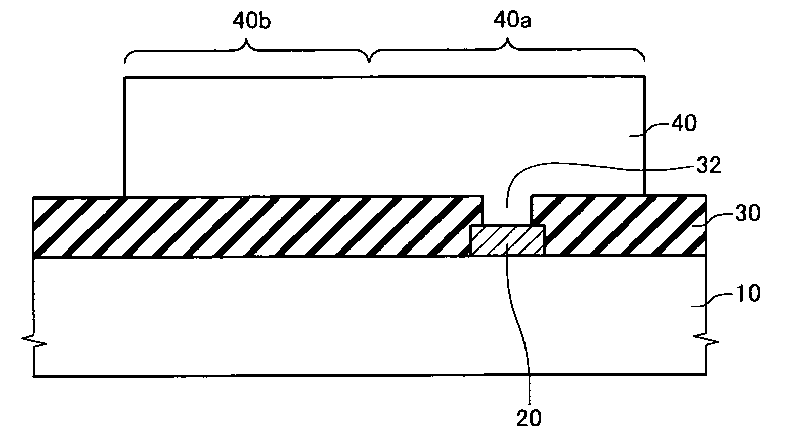
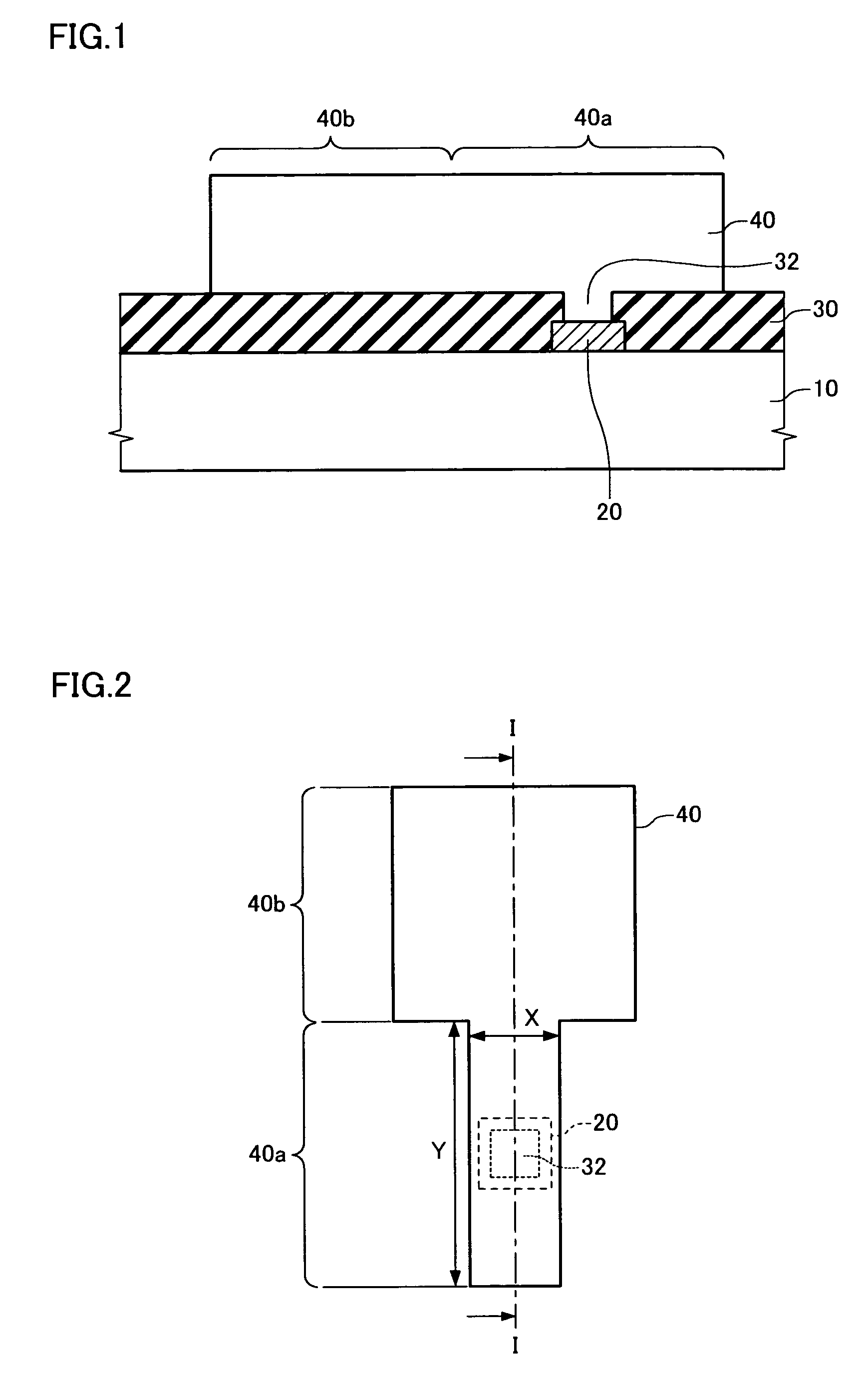
[0053] A semiconductor device according to a first embodiment is described below with reference to FIGS. 1 and 2. FIG. 1 is a cross-sectional view schematically showing the semiconductor device according to the first embodiment, and FIG. 2 is a plan view showing the planar shape of a metal electrode included in the semiconductor device shown in FIG. 1. Note that FIG. 1 is a cross-sectional view along the line I-I shown in FIG. 2.

[0054] As shown in FIG. 1, the semiconductor device according to the first embodiment includes a base 10. The base 10 may be a silicon substrate or the like. An integrated circuit (not shown) may be formed on the silicon substrate. The base 10 may be in the shape of a chip, or may be a semiconductor wafer.

[0055] An electrode pad 20 having a specific pattern is formed on the base 10. The electrode pad 20 may be electrically connected with the integrated circuit formed on the base 10. The electrode pad 20 may be formed of a metal ...

second embodiment

[0069] 1.2. Second Embodiment

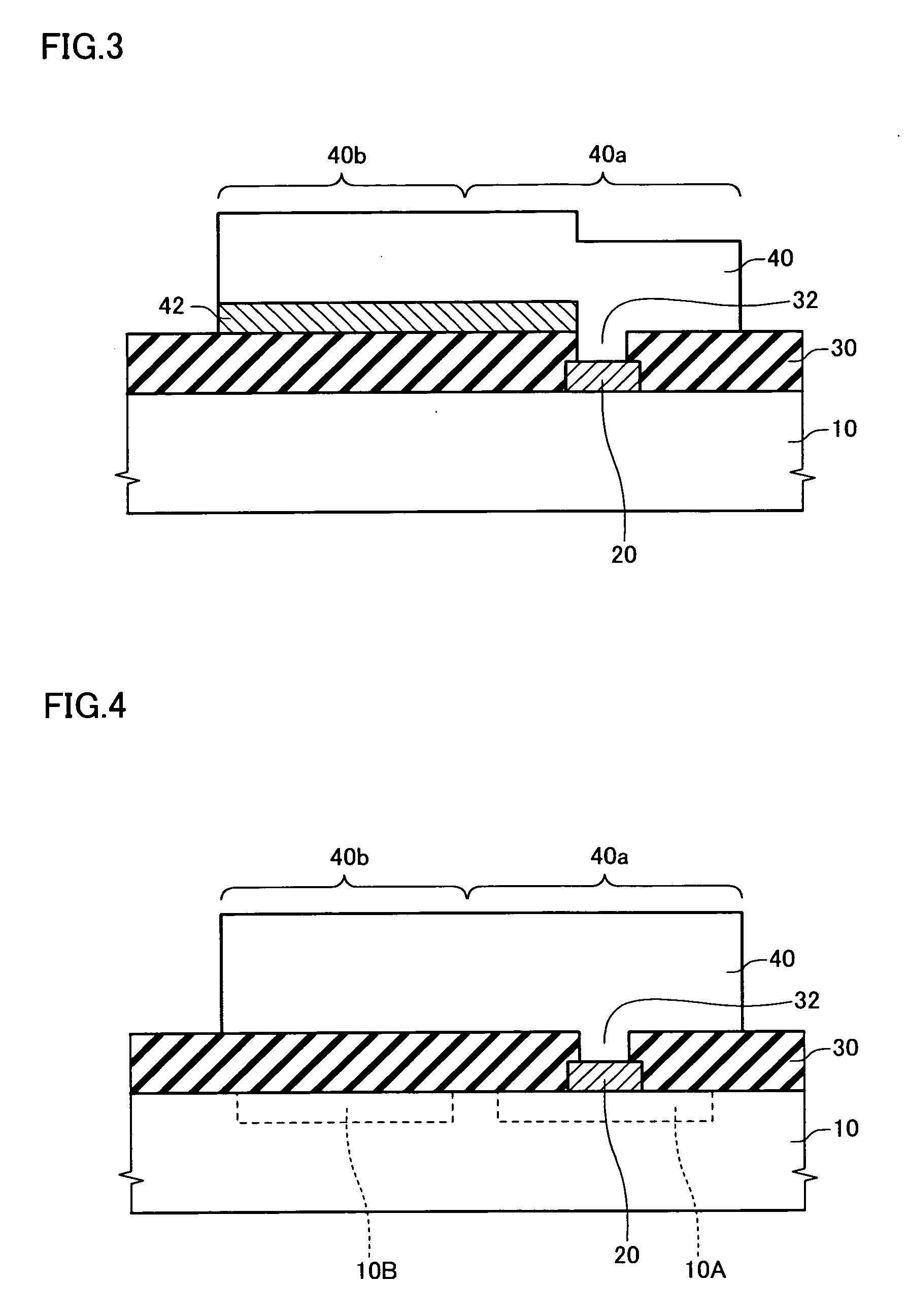
[0070] A semiconductor device according to a second embodiment is described below with reference to FIG. 4. FIG. 4 is a cross-sectional view schematically showing the semiconductor device according to the second embodiment. Note that detailed description of the same configurations and members as in the first embodiment is omitted.

[0071] As shown in FIG. 4, the semiconductor device according to the second embodiment includes the base 10, the electrode pad 20 provided above the base 10, the insulating layer 30 provided on the electrode pad 20 and having the opening 32, and the metal electrode 40. In the semiconductor device according to the second embodiment, a forbidden region 10A is provided under the first portion 40a of the metal electrode 40, and an element formation region 10B is provided under the second portion 40b. The forbidden region 10A is a region in which a semiconductor element is not formed, and the element formation region 10B is a region...

third embodiment

[0074] 2.1. Third Embodiment

[0075] A semiconductor chip according to a third embodiment is described below with reference to FIGS. 5A and 5B. FIG. 5A is a cross-sectional view schematically showing the semiconductor chip according to the third embodiment, and FIG. 5B is an enlarged plan view showing the section A shown in FIG. 5A. In the semiconductor chip according to the third embodiment, the metal electrodes 40 described in the first embodiment are arranged. The cross-sectional structure and the planar shape of the metal electrode 40 are the same as described in “1.1. First embodiment”.

[0076] In a semiconductor chip 100 according to the third embodiment, the metal electrodes 40 are arranged along the edge of the long side, as shown in FIG. 5A. As shown in FIG. 5B, the metal electrodes 40 are arranged so that the first portion 40a and the second portion 40b of the adjacent metal electrodes 40 are not disposed side by side. In more detail, the first portion 40a of one metal electr...


PUM


Abstract

A semiconductor device including: a semiconductor layer; an electrode pad provided above the semiconductor layer; an insulating layer provided above the electrode pad and having an opening which exposes at least part of the electrode pad; and a metal electrode provided at least in the opening and including a first portion provided above the electrode pad, and a second portion provided above part of the insulating layer positioned outside the electrode pad, an area of a top surface of the second portion being larger than an area of a top surface of the first portion.

Description

[0001] Japanese Patent Application No. 2005-225450, filed on Aug. 3, 2005, is hereby incorporated by reference in its entirety. BACKGROUND OF THE INVENTION [0002] The present invention relates to a semiconductor device and a semiconductor chip. [0003] In a semiconductor chip, electrode pads connected with an internal circuit are generally provided along the edge of the semiconductor chip. A technology has been known in which bumps are provided on the electrode pads and electrically connected with an interconnect pattern of a substrate in a state in which the bumps face the substrate (JP-A-9-237800, for example). [0004] In recent years, the area of the electrode pad has been reduced along with a reduction in size of the semiconductor chip. Therefore, the size of the bump is also reduced, whereby the area of the mounting surface is decreased. A decrease in the area of the mounting surface may impair reliable electrical connection with the interconnect pattern of the substrate. Moreove...

Claims


Application Information

Patent Timeline
Patent Type & Authority Applications(United States)
IPC IPC(8): H01L23/48
CPCH01L24/05H01L2924/13091H01L2224/05552H01L2224/05644H01L2224/05647H01L2224/05655H01L2224/4943H01L2924/01004H01L2924/01005H01L2924/01013H01L2924/01014H01L2924/01022H01L2924/01028H01L2924/01029H01L2924/01033H01L2924/01074H01L2924/01079H01L2924/14H01L2924/19043H01L24/06H01L2924/01006H01L2924/00014H01L2924/00012H01L2924/00H01L2224/023H01L2224/49431H01L2924/0001
Inventor SHINDO, AKINORITAKANO, MICHIYOSHI
Owner SEIKO EPSON CORP
Why Eureka
Try Eureka