Semiconductor device and fabrication method therefor

a semiconductor device and semiconductor technology, applied in the field of stacking semiconductor devices, can solve the problems of increasing costs, increasing costs, and disadvantages of downsizing, and achieve the effects of reducing the height of the semiconductor device, reducing the size and the cost, and excellent quality

Active Publication Date: 2007-03-01
VALLEY DEVICE MANAGEMENT
View PDF7 Cites 12 Cited by
  • Summary
  • Abstract
  • Description
  • Claims
  • Application Information

AI Technical Summary

Benefits of technology

[0012] The present invention has been made in view of the above circumstances and provides a semiconductor device in which the size and the costs can be reduced and the quality is excellent and a fabrication method therefor.
[0013] According to a first aspect of the present invention, there is provided a semiconductor device including: a first semiconductor chip disposed on a substrate; a first sealing resin sealing the first semiconductor chip; a built-in semiconductor device disposed on the first sealing resin; and a second sealing resin sealing the first sealing resin and the built-in semiconductor device and covering a side surface of the substrate. According to an aspect of the present invention, it is possible to prevent the second sealing resin from peeling off between the substrate and the second sealing resin, due to the mechanical stress, temperature change, and moisture change. Also, it is possible to reduce the height of the semiconductor device and downsize the semiconductor device. Accordingly, it is possible to provide a high-quality semiconductor device that can be downsized.
[0014] According to a second aspect of the present invention, there is provided a method of fabricating semiconductor device including: disposing first semiconductor chips on a substrate; sealing the first semiconductor chips by first sealing resins; cutting the substrate between the first sealing resins to form divided substrates; disposing divided substrates on a dummy sheet; forming a second sealing resin sealing built-in semiconductor devices disposed on the first sealing resins, and covering dummy sheet between the first sealing resins; and cutting the second sealing resin between the first sealing resins. According to an aspect of the present invention, it is possible to reduce the height of the semiconductor device and downsize the semiconductor device. Accordingly, it is possible to provide a high-quality semiconductor device that can be downsized.

Problems solved by technology

Unless the semiconductor chip 86 is tested, the subsequent fabrication process is performed on a defective semiconductor chip 86, thereby increasing the costs.
In this manner, there are disadvantages in downsizing.
For this reason, when the sealing resin 168 is provided, it is difficult to fill the sealing resin between the relay substrate 140 and the relay substrate 150, and it is likely to result in voids.
This increases the costs.

Method used


Image

  • Semiconductor device and fabrication method therefor
  • Semiconductor device and fabrication method therefor
  • Semiconductor device and fabrication method therefor

Examples


first embodiment

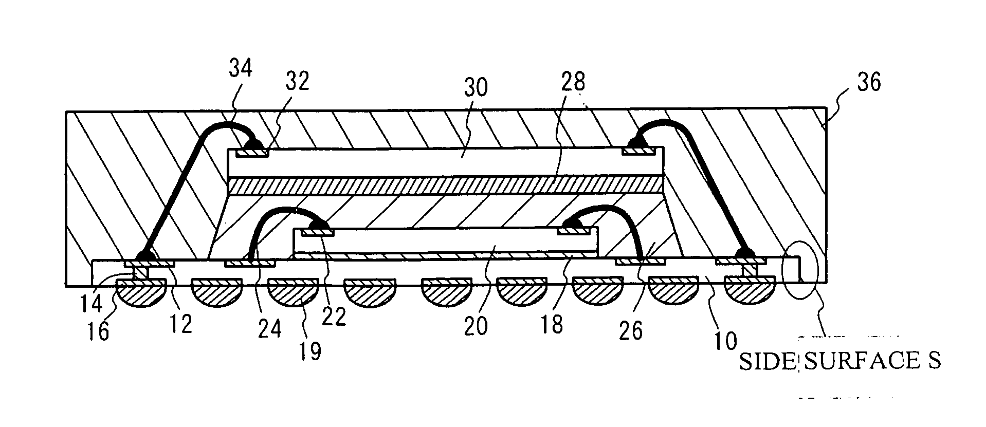
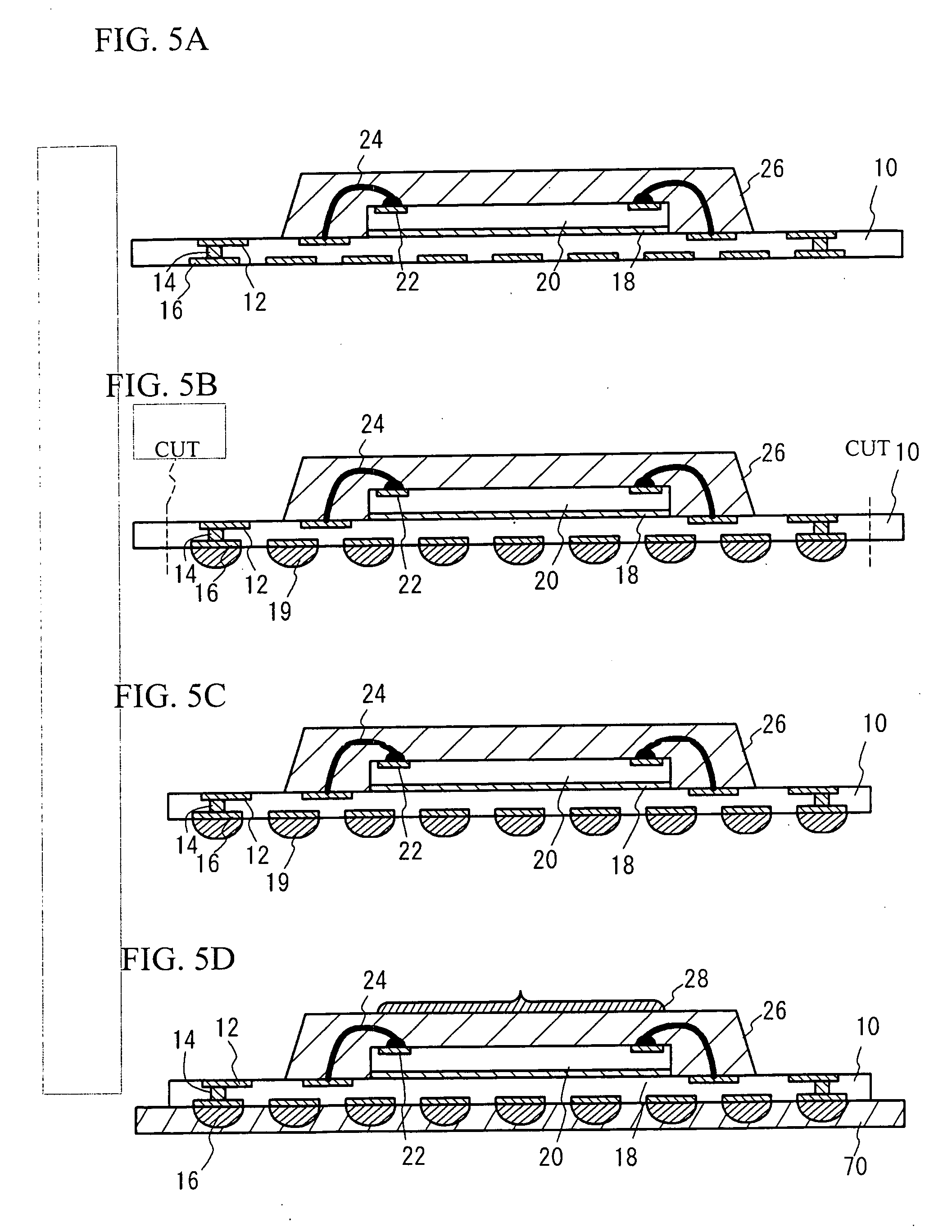
[0035]FIG. 4 is a cross-sectional view of a semiconductor device in accordance with a first embodiment of the present invention. There is disposed a first semiconductor chip 20, which is firmly attached on a relay substrate 10 (substrate) by using a die attach material 18. Pad electrodes 22 of the first semiconductor chip 20 are electrically coupled to pad electrodes 12 of the relay substrate 10 by wires 24. The first semiconductor chip 20 is sealed with a first sealing resin 26. There is disposed a semiconductor chip 30 (built-in semiconductor device), which is attached on the first sealing resin 26 by using an adhesive 28. Pad electrodes 32 of the second semiconductor chip 30 are electrically coupled to the pad electrodes 12 of the relay substrate 10 by wires 34. The first sealing resin 26 and the second semiconductor chip 30 are sealed with a second sealing resin 36. In addition, side surfaces S of the relay substrate 10 are covered with the second sealing resin 36. The relay sub...

second embodiment

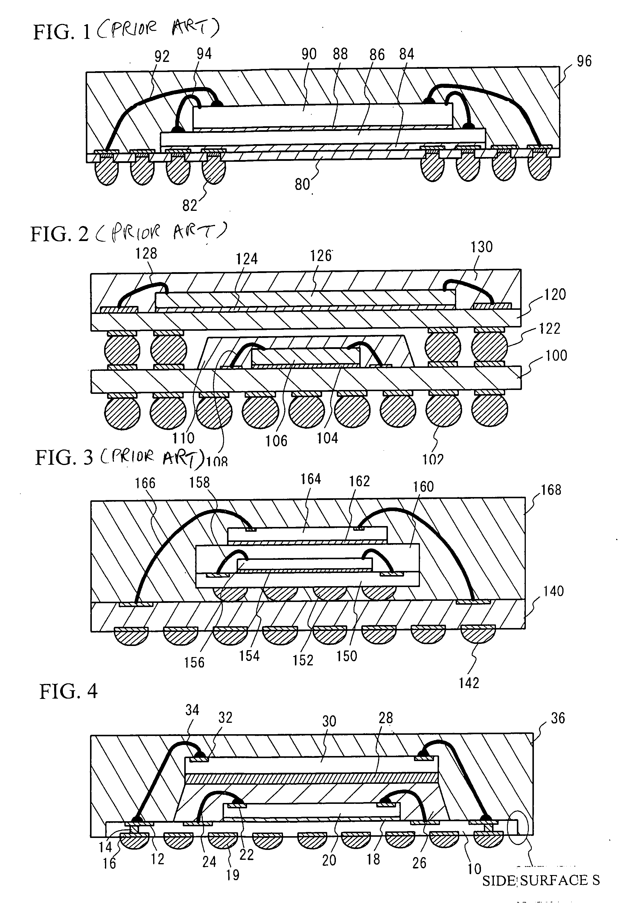
[0044]FIG. 7 is a cross-sectional view of a semiconductor device in accordance with a second embodiment of the present invention. The same components and configurations as those employed in the first embodiment have the same reference numerals and a detailed explanation will be omitted. In the second embodiment, the pad electrodes 32 of the second semiconductor chip 30 are wire bonded to the pad electrodes 12 of the relay substrate 10 from the pad electrodes 12 to the pad electrodes 32 (reverse bonding). So, wires 34a can be lower than those employed in the first embodiment. Accordingly, the second sealing resin 36 can be lower and the semiconductor device can be downsized.

third embodiment

[0045]FIG. 8 is a cross-sectional view of a semiconductor device in accordance with a third embodiment of the present invention. In the third embodiment, a semiconductor device 50 having a second semiconductor chip 45 built therein is mounted, instead that the second semiconductor chip 30 employed in the first embodiment is directly provided. Other configurations are same as those employed in the first embodiment, and the same components and configurations as those employed in the first embodiment have the same reference numerals and a detailed explanation will be omitted. Referring to FIG. 8, in the built-in semiconductor device 50, the second semiconductor chip 45 is firmly attached onto (below, in the drawing) the relay substrate 40 by using a die attach material 48. The second semiconductor chip 45 and pad electrodes 42 of the relay substrate 40 are connected by wires 44. The second semiconductor chip 45 is sealed with a third sealing resin 46. The built-in semiconductor device ...


PUM


Abstract

The present invention provides a semiconductor device and a fabrication method therefor, the semiconductor device including a first semiconductor chip (20) disposed on a substrate (10), a first sealing resin (26) sealing the first semiconductor chip (20), a built-in semiconductor device (30) disposed on the first sealing resin (26), and a second sealing resin (36) sealing the first sealing resin (26) and the built-in semiconductor device (30) and covering a side surface (S) of the substrate (10). According to an aspect of the present invention, it is possible to provide a high-quality semiconductor device and a fabrication method therefor, in which downsizing and cost reduction can be realized.

Description

CROSS-REFERENCES TO RELATED APPLICATIONS [0001] This is a continuation in part of International Application No. PCT / JP2005 / 015694, filed Aug. 30, 2005 which was not published in English under PCT Article 21(2). TECHNICAL FIELD [0002] This invention relates generally to semiconductor devices and fabrication methods therefor, and more particularly, to a stacked semiconductor device in which multiple semiconductor chips are mounted in a package and a fabrication method therefor. BACKGROUND DESCRIPTION OF THE RELATED ART [0003] In recent years, downsizing is demanded for semiconductor devices for use in non-volatile memories of mobile electronics devices such as mobile telephones and IC memory cards. For downsizing, there is a need for packaging technology that the semiconductor chips are efficiently packaged. [0004]FIG. 1 (PRIOR ART) is a cross-sectional view showing a Multi Chip Package (MCP) of Conventional Example 1. Referring to FIG. 1 (PRIOR ART), a semiconductor chip 86 is firmly...

Claims


Application Information

Patent Timeline
Patent Type & Authority Applications(United States)
IPC IPC(8): H01L23/29
CPCH01L21/568H01L2224/48091H01L23/3128H01L23/3135H01L23/66H01L25/0657H01L25/18H01L2221/68331H01L2223/6677H01L2224/32145H01L2224/32225H01L2224/48145H01L2224/48227H01L2224/48465H01L2224/48471H01L2224/48479H01L2224/73265H01L2224/85051H01L2224/85986H01L2225/0651H01L2924/01004H01L2924/01078H01L2924/14H01L2924/15311H01L2924/15331H01L2924/19107H01L21/6835H01L21/56G06F1/183H01L2924/01019H01L2224/85186H01L2924/00H01L2924/00012H01L2924/00014H01L2924/181H01L24/73H01L24/48H01L2224/45099H01L2224/4554H01L21/563H01L24/11H01L24/85H01L25/50H01L2225/0652H01L2225/06548H01L2225/06568H01L2225/06575H01L2225/06586
Inventor ONODERA, MASANORIMEGURO, KOUICHITANAKA, JUNJI
Owner VALLEY DEVICE MANAGEMENT
Why Eureka
Try Eureka