Led lens for backlight

a technology of led lenses and backlights, which is applied in the direction of instruments, lighting and heating apparatus, semiconductor devices for light sources, etc., can solve the problems of reducing the efficiency of backlight luminance, and reducing the thickness of backlights. , to achieve the effect of reducing the thickness of backlights, increasing the efficiency of backlight luminance, and reducing the amount of light radiated in the vertical direction

Active Publication Date: 2007-03-01
SAMSUNG ELECTRONICS CO LTD
View PDF7 Cites 77 Cited by
  • Summary
  • Abstract
  • Description
  • Claims
  • Application Information

AI Technical Summary

Benefits of technology

[0017] Furthermore, the amount of light radiated in the vertical direction of the lens body is more than 10% of the amount of light emitted from the LED light source. It is preferred that the amount of light radiated in the vertical direction may be adjusted according to the requirements of a backlight. In more detail, when it is desired to reduce the thickness of a backlight, the amount of light is adjusted to approach 10% of the amount of the emitted light. When it is desired to increase the efficiency of backlight luminance, the amount of light radiated in the vertical direction is adjusted to increase.

Problems solved by technology

This light results in erroneous light in the lens.
Such erroneous light degrades the performance of the overall system and the uniformity of color and luminance, therefore it may act as a factor that can increase the thickness of the overall system.
This can also degrade the overall performance of the light.
However, although, in such a scheme, improvement in the efficiency of the overall system may be expected, there is a problem in which luminance variation among individual light sources causes non-uniformity of the overall system because the backlight system is not constructed using only a single light source.
In contrast, in a system in which a plurality of LED light sources is arranged, a problem occurs in that the overall luminance is non-uniform because the light beams emitted from respective light sources overlap or have spacing intervals therebetween.

Method used


Image

  • Led lens for backlight
  • Led lens for backlight
  • Led lens for backlight

Examples


Embodiment Construction

[0029] Preferred embodiments of the present invention are described with reference to the accompanying drawings below.

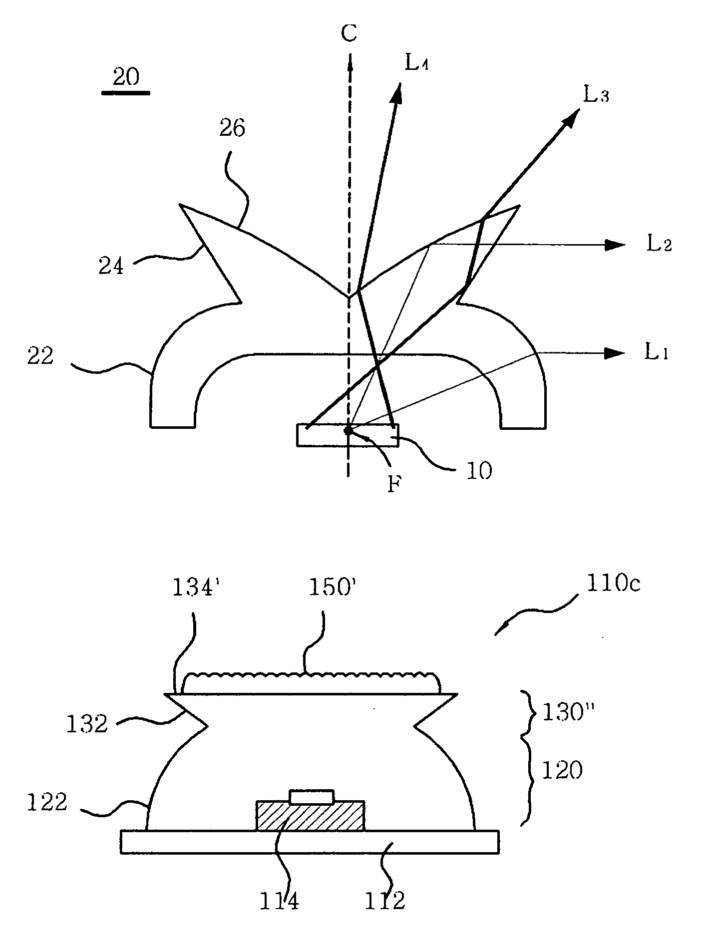
[0030]FIG. 3 is a diagram showing an LED lens according to an embodiment of the present invention. The LED lens of FIG. 3 includes an LED light source 114 formed on a substrate 112, a lower body 120 configured to accommodate the LED light source in the lower portion thereof, an upper body 130 formed on the lower body, and a beam shaping element 150 fastened to the top of the upper body 130.

[0031] The lower body 120 accommodates the LED light source 114 in the lower portion thereof, and has a lower refracting surface 122 that is formed to be symmetrical with respect to a central axis C. An upper refracting surface 132 is connected to the front end of the lower refracting surface 122 to be symmetrical with respect to the central axis C, and an upper reflecting surface 134 is disposed to form a predetermined angle from the front end of the upper refracting surface 132...


PUM


Abstract

Disclosed herein is a Light Emitting Diode (LED) lens for a backlight. The LED lens includes an LED light source, a lens body, and a beam shaping element. The lens body is configured such that the LED light source is accommodated in the lower portion thereof, and light emitted from the LED light source is radiated in vertical and lateral directions of the lens body. The beam shaping element is fastened to the top of the lens body and is configured to adjust light beams radiated through the upper surface of the lens body. Accordingly, the uniformity of luminance and color can be increased and, at the same time, the overall performance of the system can be improved.

Description

BACKGROUND OF THE INVENTION [0001] 1. Field of the Invention [0002] The present invention relates generally to a light emitting diode lens for a backlight and, more particularly, to a light emitting diode lens for a backlight, which radiates light, emitted from a light emitting diode light source, in lateral and vertical directions of a lens body, thus improving the uniformity of luminance and color in the overall system to which the LED lens is applied. [0003] 2. Description of the Related Art [0004] Recently, in a display device and an illumination optical system, demands for a light source having environment-friendliness, high efficiency and a long lifespan are increasing. Furthermore, as the efficiency and luminance of a Light Emitting Diode (LED) are increasing continuously, an alternative light source using an LED has been developed and is gradually being applied to the display device and the illumination optical system. In particular, as projects, such as the development of a...

Claims


Application Information

Patent Timeline
Patent Type & Authority Applications(United States)
IPC IPC(8): F21V7/00
CPCF21V5/04F21V7/0091F21Y2101/02G02B19/0061H01L33/60G02B19/0071G02B19/0028H01L33/54F21V17/002F21Y2115/10G02F1/1335
Inventor KIM, JIN JONGJEONG, HO SEOP
Owner SAMSUNG ELECTRONICS CO LTD
Why Eureka
Try Eureka