
Reference voltage generating circuit, a semiconductor integrated circuit and a semiconductor integrated circuit apparatus

a reference voltage and semiconductor technology, applied in the direction of electric variable regulation, process and machine control, instruments, etc., can solve the problem that the offset voltage between input terminals of differential amplifiersb>0/b> cannot be ignored, and achieve the effect of accurate output voltag

Inactive Publication Date: 2007-03-08
RENESAS ELECTRONICS CORP
View PDF5 Cites 34 Cited by
  • Summary
  • Abstract
  • Description
  • Claims
  • Application Information

AI Technical Summary

Benefits of technology

[0013] An object of the present invention is to provide a band gap type reference voltage generating circuit and a semiconductor integrated circuit having the same, capable of generating a reference voltage of about 1.2V or less subjected to temperature compensation and power supply voltage compensation, and reducing the offset voltage dependency of the differential amplifier.
[0019] Preferably, a resistor is connected in parallel with the resistor and the diode for current-voltage conversion in the output part. More preferably, a startup circuit is provided which has a function of receiving / passing current from / to the first or second resistor in the band gap part on start of operation of the reference voltage generating circuit and, after the output of the differential amplifier rises to a predetermined level, interrupting the receiving current or passing current. With the configuration, a situation such that the reference voltage generating circuit becomes stable in a state other than a state where a desired output voltage is output is avoided, and accurate output voltage can be obtained.
[0021] According to the invention, the band gap type reference voltage generating circuit capable of generating a reference voltage of about 1.2V or less subjected to temperature compensation and power supply voltage compensation and achieving reduced offset voltage dependency of a differential amplifier can be realized.

Problems solved by technology

In the case of attempting to obtain a high-precision reference voltage, however, an offset voltage between input terminals of the differential amplifier AMP0 cannot be ignored.

Method used


Image

  • Reference voltage generating circuit, a semiconductor integrated circuit and a semiconductor integrated circuit apparatus
  • Reference voltage generating circuit, a semiconductor integrated circuit and a semiconductor integrated circuit apparatus
  • Reference voltage generating circuit, a semiconductor integrated circuit and a semiconductor integrated circuit apparatus

Examples


first embodiment

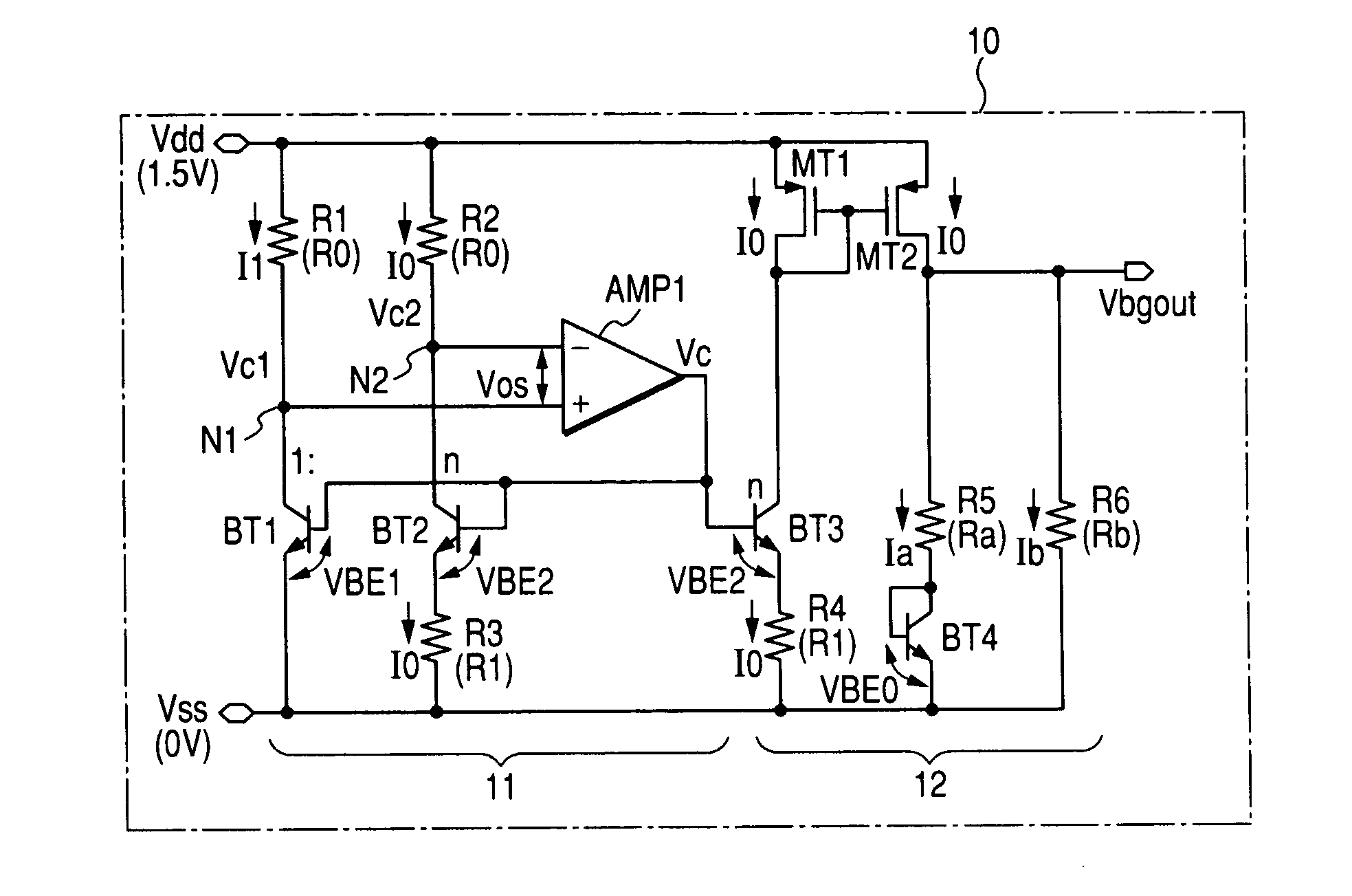
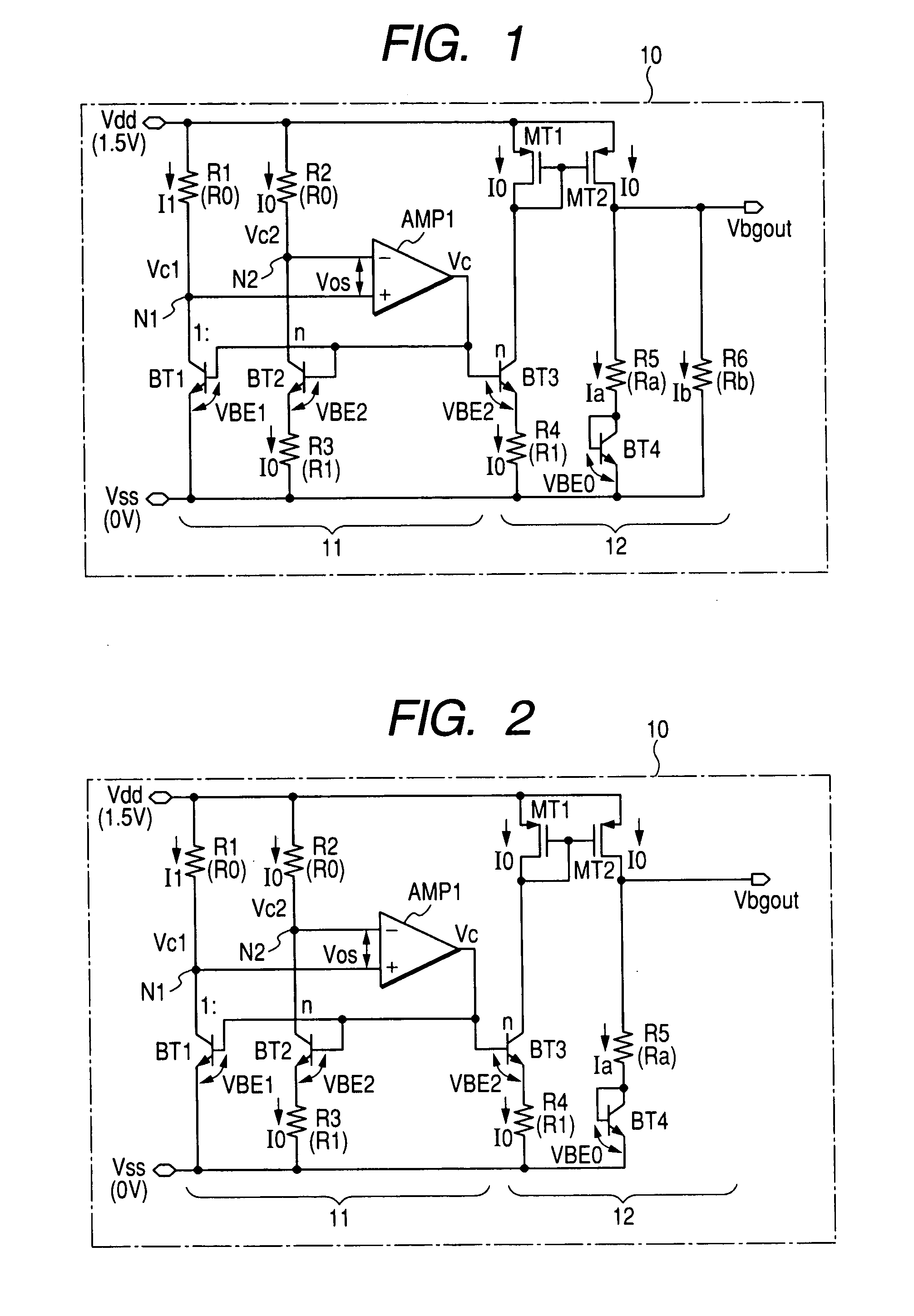
[0036]FIG. 1 shows a reference voltage generating circuit according to the present invention.

[0037] The reference voltage generating circuit shown in the diagram has a resistor R1 and an NPN bipolar transistor BT1 connected in series between a power supply terminal to which a power supply voltage Vdd such as 1.5V is applied and a power supply terminal to which a power supply voltage Vss such as a ground potential (0V) is applied. The reference voltage generating circuit also has a resistor R2, an NPN bipolar transistor BT2, and a resistor R3 connected in series between the power supply terminals. The resistors R1 and R2 have the same resistance value R0. The transistors BT1 and BT2 are set so that the emitter size has a ratio of 1:n. As the value of “n”, for example, “10” is selected. In place of setting the emitter size to 1:n, as the transistor BT2, n pieces of transistors of the same size as that of the transistor BT1 may be connected in parallel.

[0038] Further, a differential a...

second embodiment

[0062] In accordance with the change, to reverse the potential relations in the embodiment of FIG. 1, the transistors BT1, BT2, and BT3 and the resistors R3 and R4 are provided on the side of the power supply voltage Vdd, and the resistors R1 and R2 and the transistors MT1 and MT2 are provided on the side of the power supply voltage Vss. Further, as the differential amplifier AMP1, a circuit using a P-channel MOS transistor as a differential input transistor is used. Since the principle of operation of the reference voltage generating circuit of the second embodiment is the same as that of the reference voltage generating circuit of the embodiment of FIG. 1, the detailed description of the operation will not be repeated.

[0063]FIG. 6 shows a modification of the reference voltage generating circuit of the second embodiment of FIG. 5. In the modification, the resistor R6 in the output part in the circuit of FIG. 5 is omitted, and the output voltage Vbgout is slightly lower than that in...

third embodiment

[0066] The reference voltage Vref generated by the resistance dividing circuit 21 is applied to the non-inversion input terminal of the differential amplifier AMP2, the potential Vc1 at the node N1 of the reference voltage generating circuit 10 is applied to the inversion input terminal of the differential amplifier AMP2. The current mirror circuit 22 is formed by a diode-connected MOS transistor MT4 whose gate and drain are coupled to each other and converting the control current Ibs to a voltage, and MOS transistors MT5 and MT6 in which the same voltage as the gate voltage of the MOS transistor MT4 is applied to the gates. In the third embodiment, the MOS transistors MT4 to MT6 are of the N-channel type.

[0067] Before the reference voltage generating circuit 10 is started, no current flows in the resistor R1, so that the potential Vc1 at the node N1 is at the Vdd level. Consequently, the output Vol of the differential amplifier AMP2 is at the low level. In the case of starting the ...


PUM


Abstract

The present invention provides a band gap type reference voltage generating circuit and a semiconductor integrated circuit having the same, capable of generating a reference voltage of about 1.2V or less whose temperature dependency is low, and realizing reduced offset voltage dependency of a differential amplifier. A band gap part has: a first resistor and a first bipolar transistor connected in series between power supply voltage terminals; a second resistor, a second bipolar transistor, and a third resistor connected in series between the power supply voltage terminals; and a differential amplifier that receives voltages generated by the first and second resistors, and an output of the differential amplifier is applied to the bases of the two transistors. The output part has a third bipolar transistor having a base to which the output of the differential amplifier is applied, a fourth resistor connected in series with the third bipolar transistor, a current mirror circuit for transferring current flowing in the third bipolar transistor, and a fifth resistor and a diode for converting the transferred current to voltage.

Description

CROSS-REFERENCE TO RELATED APPLICATION [0001] The present application claims priority from Japanese patent applications No. 2006-168393 filed on Jun. 19, 2006, and No. 2005-258870 filed on Sep. 7, 2005, the contents of which are hereby incorporated by reference into this application. BACKGROUND OF THE INVENTION [0002] The present invention relates to a technique for generating a reference voltage of a semiconductor integrated circuit and, more particularly, to a band gap type reference voltage generating circuit which operates on a low power supply voltage. The invention relates to a technique effectively applied to a reference voltage generating circuit for generating a reference voltage necessary for, for example, an A / D converter or a D / A converter. [0003] Since a reference voltage is necessary for a converting operation in an A / D converter or a D / A converter, a semiconductor integrated circuit having therein an A / D converter or a D / A converter is provided with a reference voltag...

Claims


Application Information

Patent Timeline
IPC IPC(8): G05F3/20
CPCG05F3/30G11C5/14
Inventor MOCHIZUKI, TOSHIOIMAIZUMI, EIKIOKUMURA, SACHIKO
Owner RENESAS ELECTRONICS CORP
Learn More