Semiconductor integrated circuit having switch circuit of digital signal
- Summary
- Abstract
- Description
- Claims
- Application Information
AI Technical Summary
Benefits of technology
Problems solved by technology
Method used
Image

Examples
Embodiment Construction
[0040] Embodiments of the present invention will be described below using the drawings. In the drawings, signal lines shown by thick lines are each composed of plural lines. Part of blocks to which the thick lines are connected are composed of plural circuits. For the signal lines to which signals are transmitted, the same numerals and symbols as the names of the signals are used.
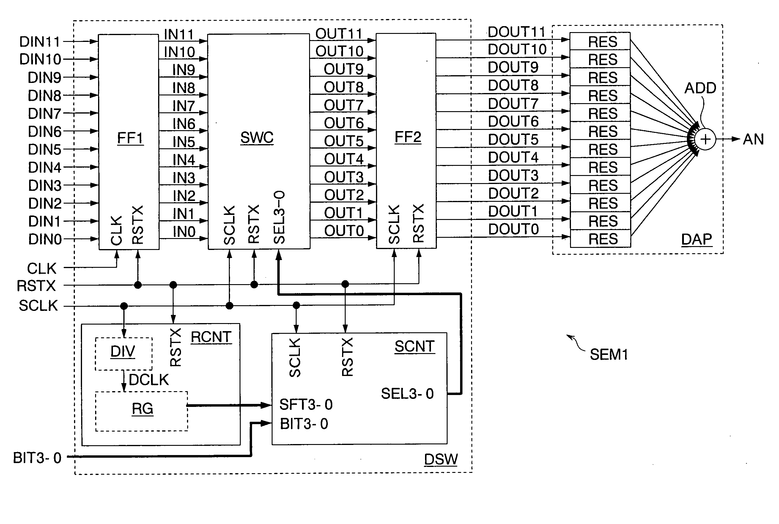
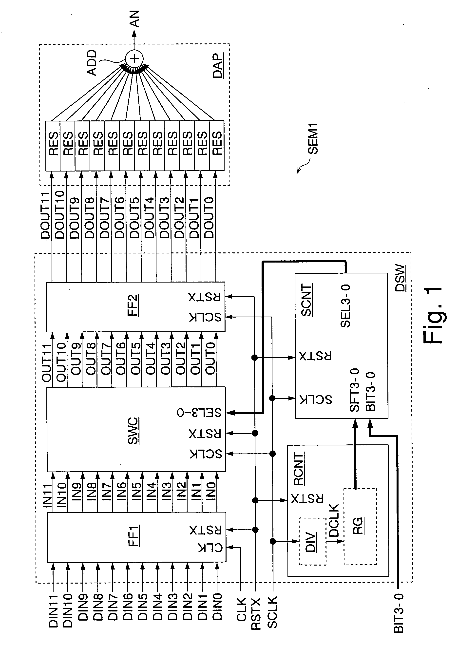
[0041]FIG. 1 shows a first embodiment of a semiconductor integrated circuit of the present invention. A semiconductor integrated circuit SEMI includes a data switching circuit DSW and a D / A conversion part DAP. For example, the semiconductor integrated circuit SEM1 is formed as a D / A converter by using a CMOS process on a silicon substrate.
[0042] The data switching circuit DSW includes a first memory unit FF1, a switch circuit SWC, a second memory unit FF2, a random-number control circuit RCNT, and a switch control circuit SCNT. The first memory unit FF1 includes 12 latches not shown, latches the value of...
PUM
 Abstract
Description
Claims
Application Information
 - Generate Ideas
- Intellectual Property
- Life Sciences
- Materials
- Tech Scout
- Unparalleled Data Quality
- Higher Quality Content
- 60% Fewer Hallucinations
Browse by: Latest US Patents, China's latest patents, Technical Efficacy Thesaurus, Application Domain, Technology Topic, Popular Technical Reports.
© 2025 PatSnap. All rights reserved.Legal|Privacy policy|Modern Slavery Act Transparency Statement|Sitemap|About US| Contact US: help@patsnap.com