

Process for cleaning wafers in an in-line cleaning process
a technology of in-line cleaning and wafers, which is applied in the direction of cleaning processes and apparatus, cleaning using liquids, chemical instruments and processes, etc., can solve the problems of deteriorating valves and having inferior stopping functions, increasing the adverse influence of affecting the product yield of semiconductor devices. achieve the effect of effectively removing the droplet of cleaning liquid
- Summary
- Abstract
- Description
- Claims
- Application Information
AI Technical Summary
Benefits of technology
Problems solved by technology
Method used
Image

Examples
Embodiment Construction
[0022] Now, the present invention is more specifically described with reference to accompanying drawings, wherein similar constituent elements are designated by similar reference numerals throughout the drawings.
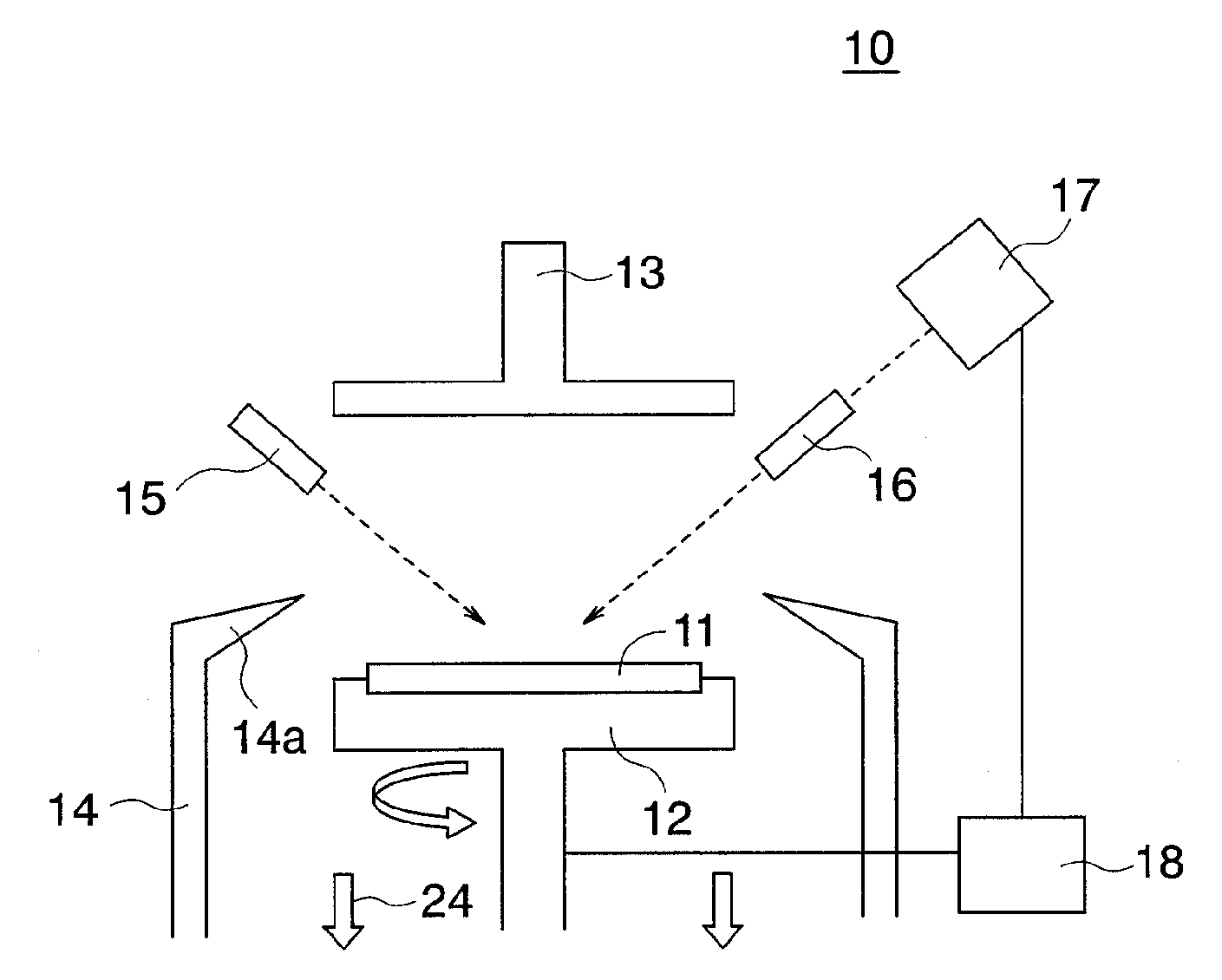
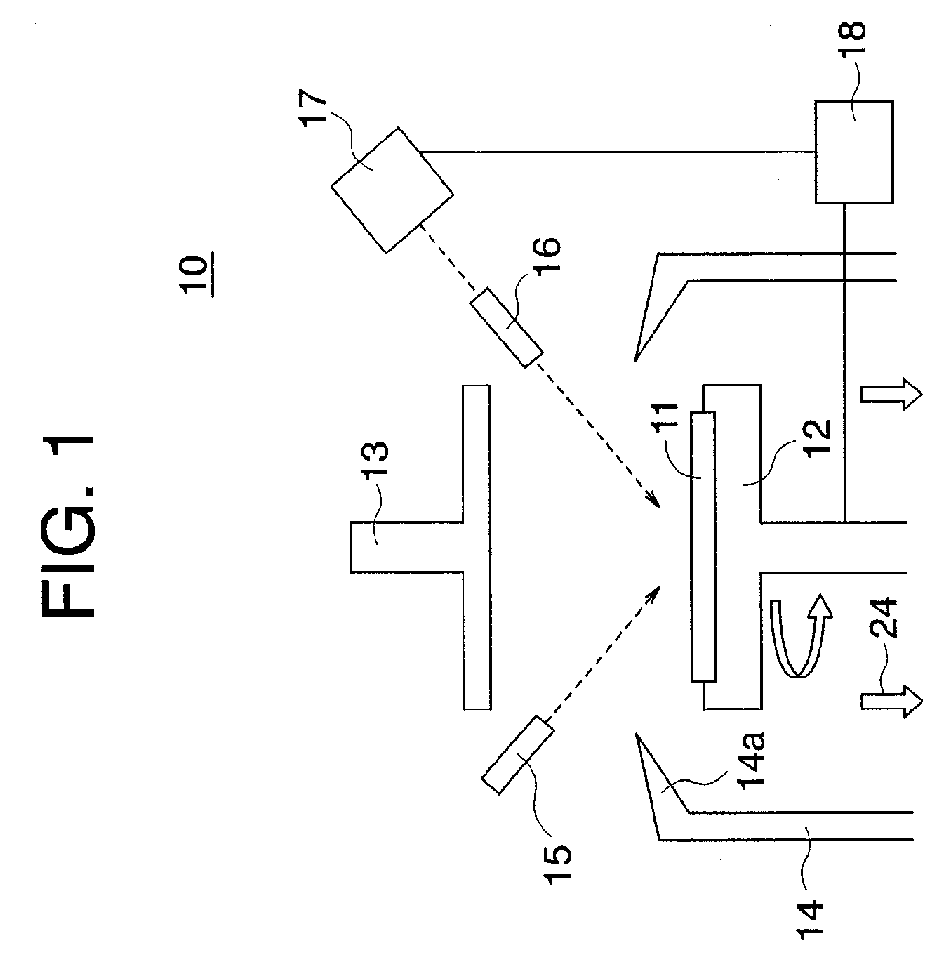
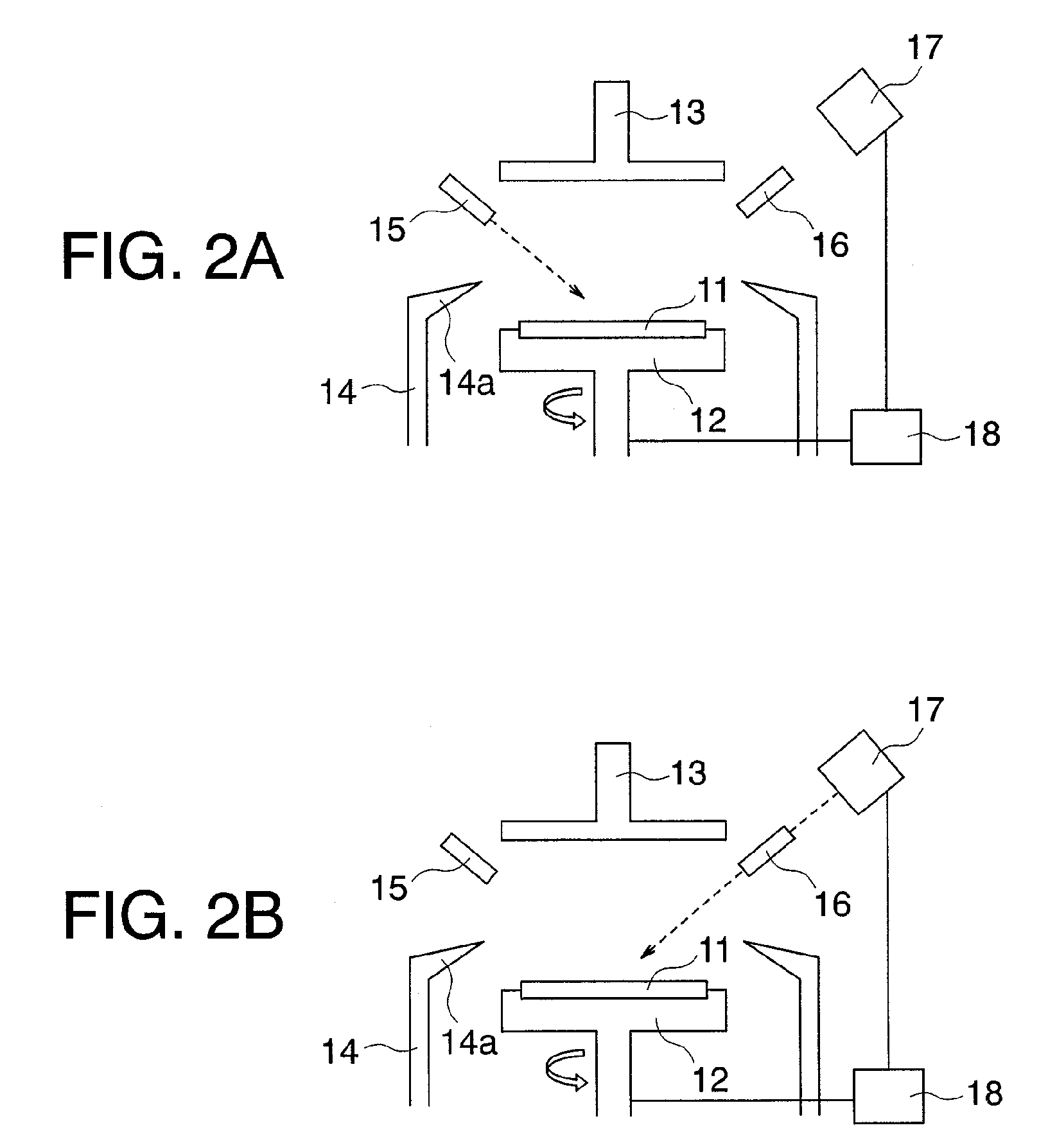
[0023]FIG. 1 shows an in-line wafer cleaning system using a wafer cleaning method according to a first embodiment of the present invention. The wafer cleaning system is used to remove polymer, for example, from the wafers one by one. The wafer cleaning system, generally designated by numeral 10, includes a wafer stage 12 for mounting thereon a wafer 11 to be cleaned, associated instrument such as nozzles 15, 16, a shield plate 13 disposed above the wafer stage 12, a guard wall 14 encircling the periphery of the wafer stage 12, sensors such as a ultra-sonic flow meter 17, and a control section including a rotational speed controller 18.
[0024] The wafer stage 12 has a protrusion on the periphery thereof for holding the wafer 11 at the periphery of the wafer 11. The wafer sta...
PUM
| Property | Measurement | Unit |
|---|---|---|
| Volume | aaaaa | aaaaa |
| Speed | aaaaa | aaaaa |
| Area | aaaaa | aaaaa |
Abstract
Description
Claims
Application Information