Scanning electron microscope and image signal processing method

a scanning electron microscope and image signal processing technology, applied in the field of scanning electron microscope, can solve the problems of not providing a means for measuring dynamic and not providing a means for adjusting the dynamic range of luminous intensity

Active Publication Date: 2007-03-22
HITACHI HIGH-TECH CORP
View PDF19 Cites 4 Cited by
  • Summary
  • Abstract
  • Description
  • Claims
  • Application Information

AI Technical Summary

Problems solved by technology

The prior art as above, however, does not provide a means for measuring the dynamic range of luminous intensity of a displa

Method used


Image

  • Scanning electron microscope and image signal processing method
  • Scanning electron microscope and image signal processing method
  • Scanning electron microscope and image signal processing method

Examples


Embodiment Construction

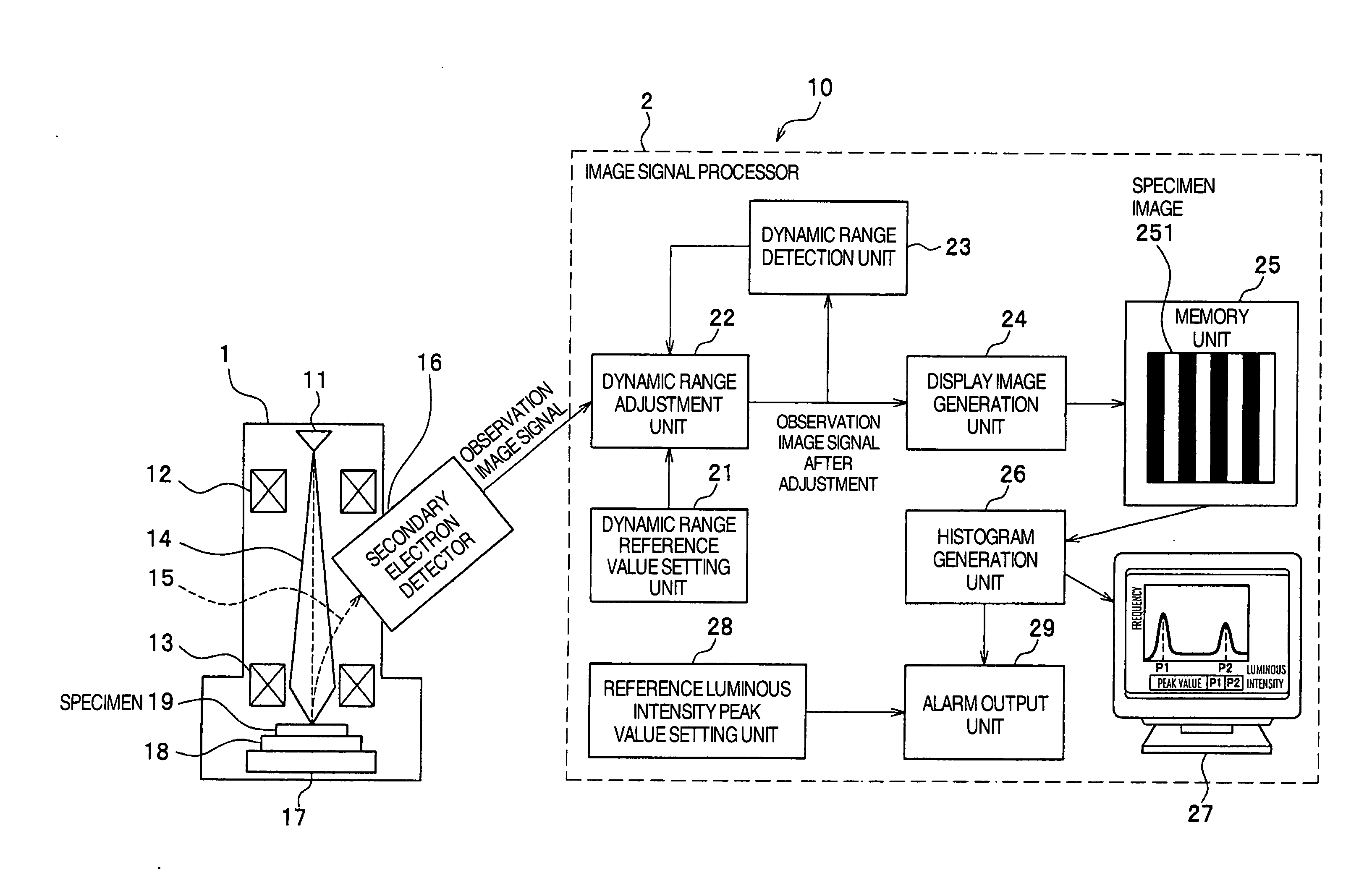
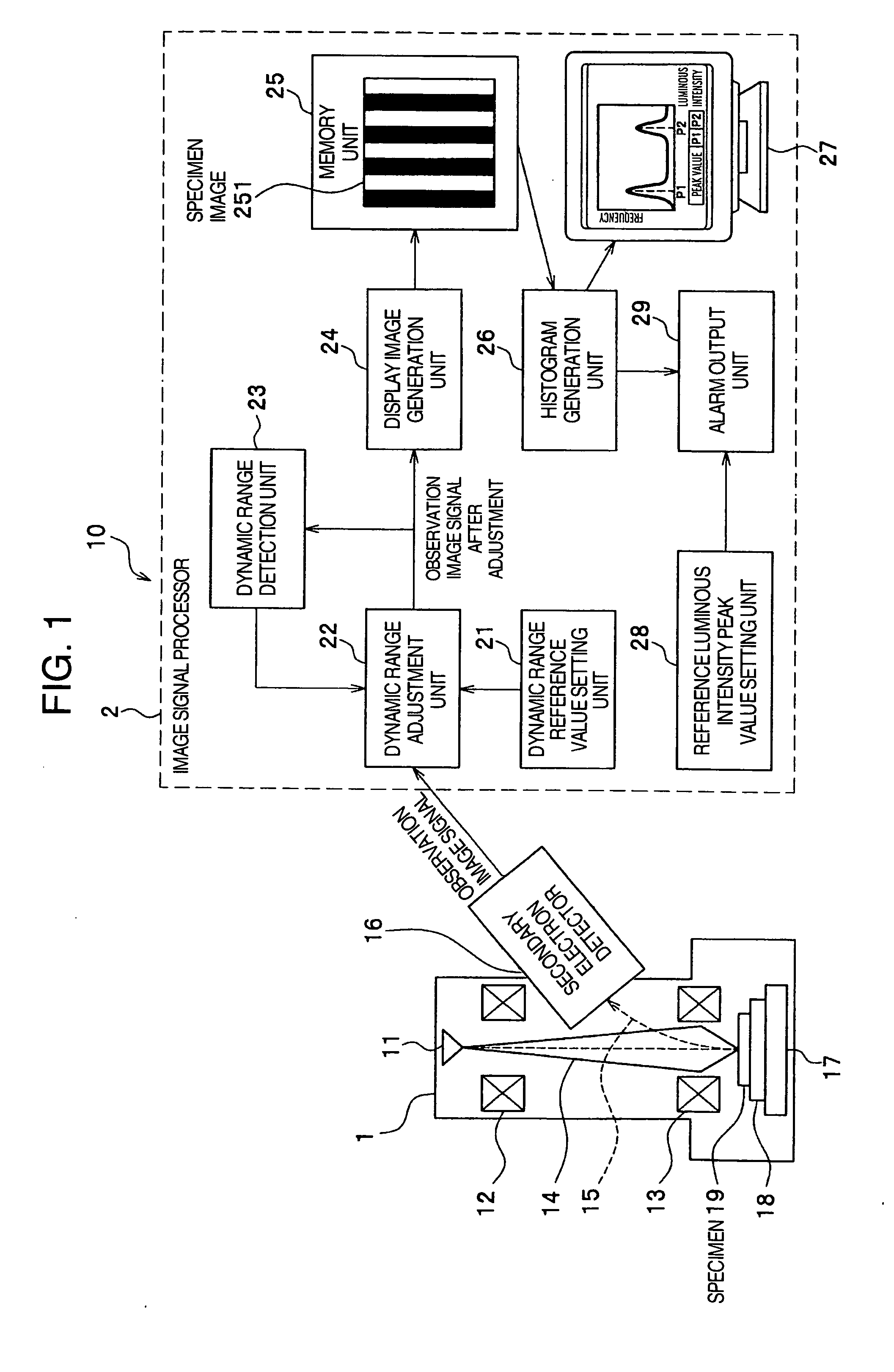
[0017] An embodiment of the present invention will now be described in greater detail by making reference to FIGS. 1 to 5 as necessary. Referring first to FIG. 1, a scanning electron microscope (SEM) according to the present embodiment is schematically constructed as illustrated therein. As shown in FIG. 1, the SEM generally designated at reference numeral 10 comprises an optics column 1 housing an electron gun 11, a condenser lens 12, an objective lens 13, a secondary electron detector 16 and an XY stage 17 and an image signal processor 2 for processing an observation image signal of specimen 19 delivered out of the secondary electron detector 16 is connected to the optics column 1.

[0018] In the optics column 1, a primary electron beam 14 emitted from the electron gun 11 is irradiated on the specimen 19 and secondary electrons 15 are discharged from a portion of specimen 19 irradiated with the primary electron beam 14. The secondary electron detector 16 detects and amplifies the s...


PUM


Abstract

The SEM has a dynamic range reference value setting unit for setting dynamic range reference values, a dynamic range adjustment unit for receiving an observation image signal delivered out of a secondary electron detector, adjusting the dynamic range of the observation image signal on the basis of the dynamic range reference values and outputting the thus adjusted observation image signal as an observation image signal after adjustment, a display image generation unit for determining luminous intensity levels of individual pixels of an image to be displayed based on the observation image signal after adjustment to generate a display image, a histogram generation unit for generating a histogram of luminous intensity levels of the display image and extracting, as a luminous intensity peak value, at which the frequency of luminous intensity is maximized, and a display unit for displaying the generated histogram and the extracted luminous intensity peak value.

Description

BACKGROUND OF THE INVENTION [0001] The present invention relates to a scanning electron microscope in which the dynamic range of luminous intensity of a display image is adjustable and an image signal processing method having the capability as above. [0002] In recent years, the scanning electron microscope (hereinafter simply referred to as SEM) has been used widely and frequently in many industrial fields including manufacture of semiconductors. When applied to industrial use, the SEM is often used mainly in the inspection process. In the SEM used in the application as such, reduction of the difference in measurement characteristics among a plurality of SEM apparatus is particularly required. [0003] When the same specimen is observed with a plurality of SEM apparatus, the luminous characteristics of displayed images, especially, their dynamic ranges need to be identical. But even if the detection sensitivity, for example, of a secondary electron detector in each of the plural SEM's...

Claims


Application Information

Patent Timeline
IPC IPC(8): H04N7/18
CPCH01J37/244H01J37/28H01J2237/24585H01J2237/2448H01J2237/221
Inventor KOBARU, ATSUSHISASADA, KATSUHIROKAWADA, HIROKI
Owner HITACHI HIGH-TECH CORP
Why Eureka
Try Eureka