Method and apparatus improving gate oxide reliability by controlling accumulated charge

a technology of metal oxide and gate oxide, applied in the field of metal oxidesemiconductor field effect transistors, can solve the problems of adversely affecting the performance of soi mosfets under certain operating conditions, adversely affecting the linearity of soi mosfets, and adversely affecting the performance of soi mosfets, so as to improve the nonlinear response and harmonic and intermodulaton distortion effects

Active Publication Date: 2007-03-29
PSEMI CORP
View PDF45 Cites 172 Cited by
  • Summary
  • Abstract
  • Description
  • Claims
  • Application Information

AI Technical Summary

Benefits of technology

[0026] Apparatuses and methods are provided to control accumulated charge in SOI MOSFETs, thereby improv...

Problems solved by technology

SOI and SOS MOSFETs are often used in applications in which operation within the accumulated charge regime adversely affects MOSFET performance.
As described below in more detail, unless the accumulated charge is removed or otherwise controlled, it detrimentally affects performance of SOI MOSFETs under certain operating conditions.
As described below with reference to FIGS. 2B and 5A in more detail, the inventors have discovered that unless the accumulated charge is removed or otherwise controlled, under some operating conditions, the accumulated charge adversely affects the linearity of the SOI MOSFET and thereby increases harmonic distortion and intermodulat...

Method used


Image

  • Method and apparatus improving gate oxide reliability by controlling accumulated charge
  • Method and apparatus improving gate oxide reliability by controlling accumulated charge
  • Method and apparatus improving gate oxide reliability by controlling accumulated charge

Examples


Embodiment Construction

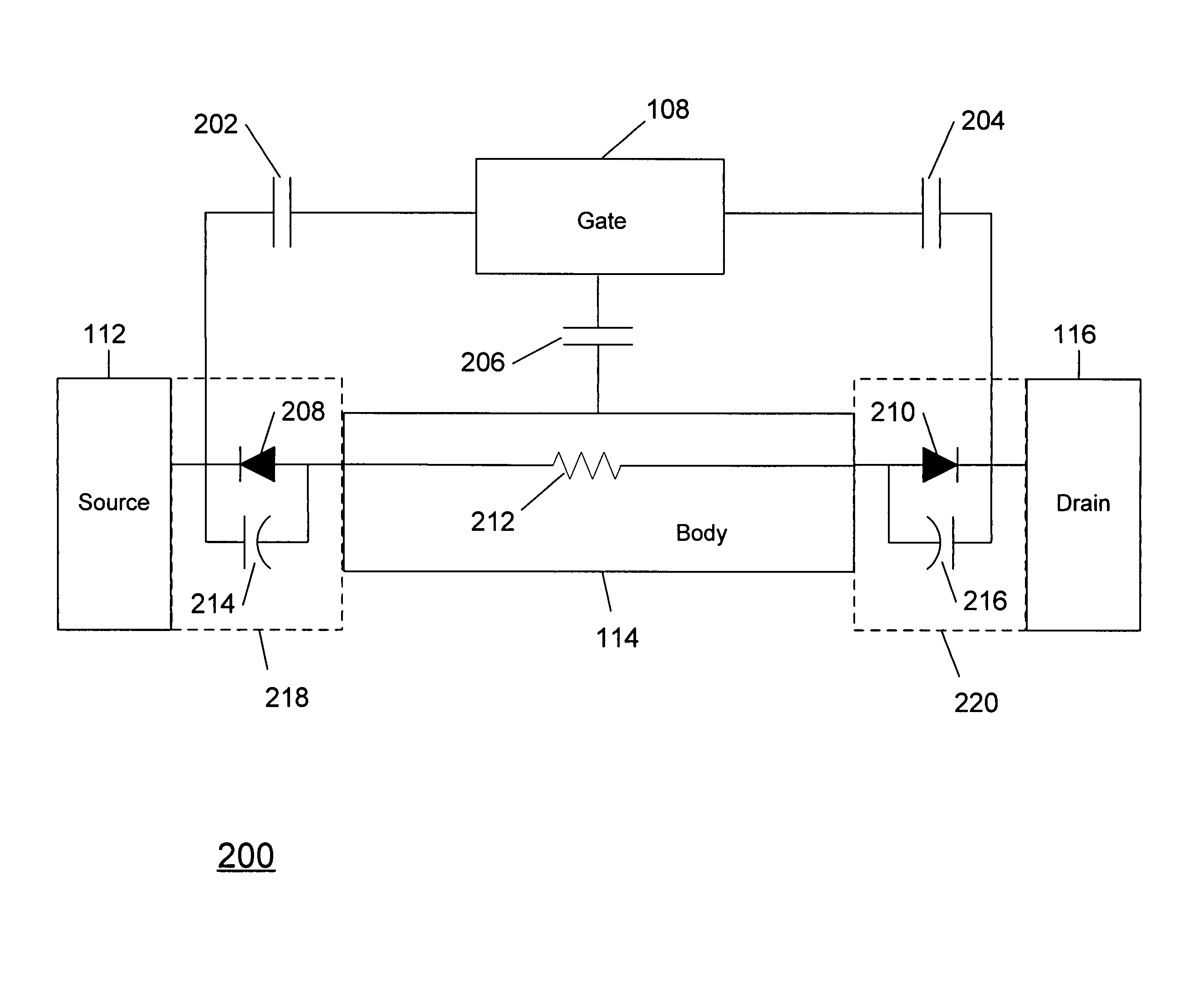
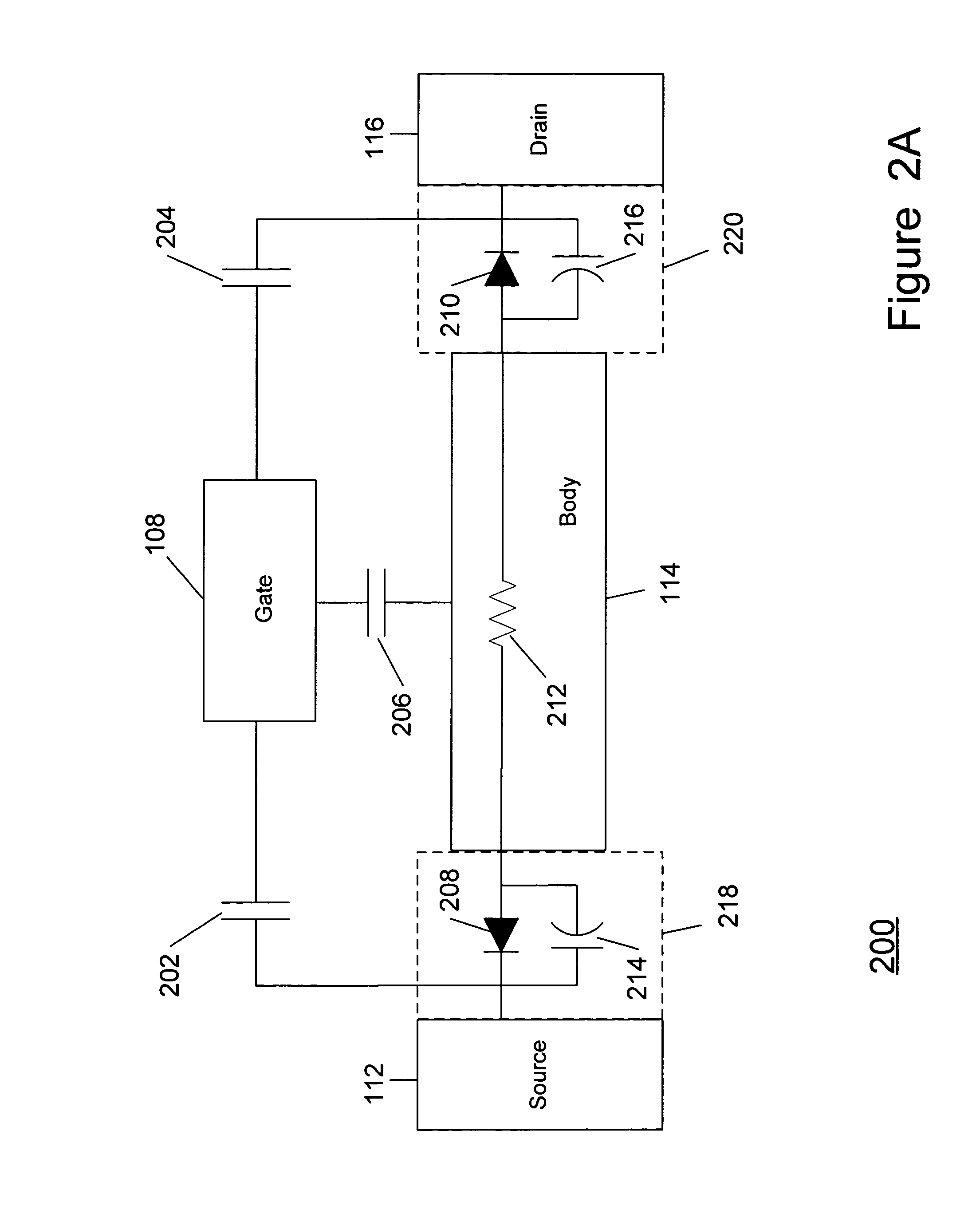
[0073] As noted above, those skilled in the electronic device design arts shall appreciate that the teachings herein apply equally to NMOSFETs and PMOSFETs. For simplicity, the embodiments and examples presented herein for illustrative purposes include only NMOSFETs, unless otherwise noted. By making well known changes to dopants, charge carriers, polarity of bias voltages, etc., persons skilled in the arts of electronic devices will easily understand how these embodiments and examples may be adapted for use with PMOSFETs.

Non-Linearity and Harmonic Distortion Effects of Accumulated Charge in an SOI NMOSFET

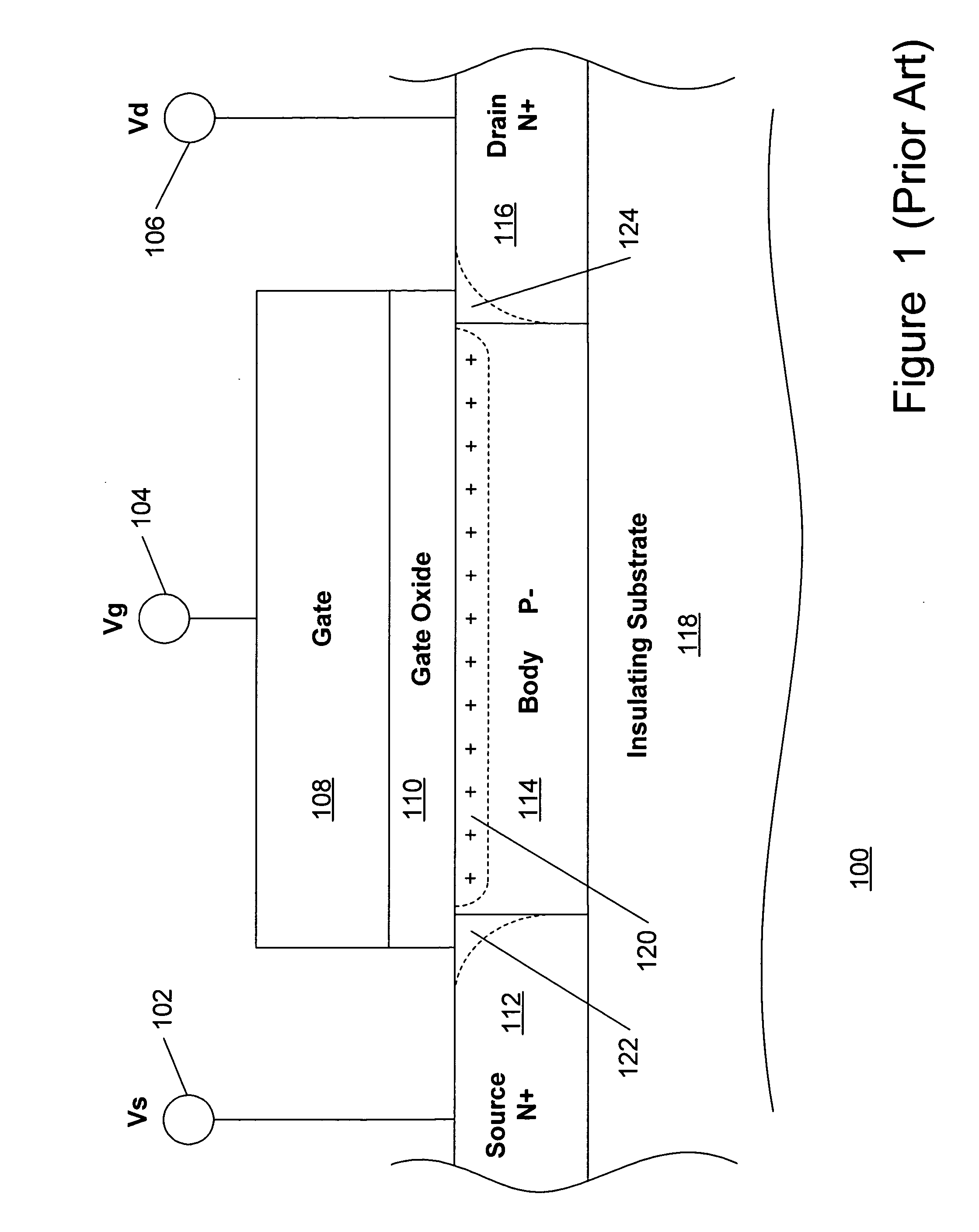
[0074] As described in the background section above, no matter what mode of operation the MOSFET employs (i.e., enhancement mode or depletion mode), under some circumstances, when a MOSFET is operated in an off-state with a nonzero gate bias voltage applied with respect to the source and drain, an accumulated charge may occur under the gate. According to the present teachings, a...


PUM


Abstract

A method and apparatus are disclosed for use in improving the gate oxide reliability of semiconductor-on-insulator (SOI) metal-oxide-silicon field effect transistor (MOSFET) devices using accumulated charge control (ACC) techniques. The method and apparatus are adapted to remove, reduce, or otherwise control accumulated charge in SOI MOSFETs, thereby yielding improvements in FET performance characteristics. In one embodiment, a circuit comprises a MOSFET, operating in an accumulated charge regime, and means for controlling the accumulated charge, operatively coupled to the SOI MOSFET. A first determination is made of the effects of an uncontrolled accumulated charge on time dependent dielectric breakdown (TDDB) of the gate oxide of the SOI MOSFET. A second determination is made of the effects of a controlled accumulated charge on TDDB of the gate oxide of the SOI MOSFET. The SOI MOSFET is adapted to have a selected average time-to-breakdown, responsive to the first and second determinations, and the circuit is operated using techniques for accumulated charge control operatively coupled to the SOI MOSFET. In one embodiment, the accumulated charge control techniques include using an accumulated charge sink operatively coupled to the SOI MOSFET body.

Description

CROSS-REFERENCE TO RELATED APPLICATIONS [0001] This application is a Continuation-in-Part (CIP) of co-pending and commonly assigned U.S. Patent application Ser. No. 11 / 484,370, filed Jul. 10, 2006, entitled “Method and Apparatus for use in Improving Linearity of MOSFETs using an Accumulated Charge Sink” (DOCKET NO. PER-016-PAP), pending, which claims the benefit under 35 U.S.C. § 119 (e) of U.S. Provisional Application No. 60 / 698,523, filed Jul. 11, 2005, entitled “Method and Apparatus for use in Improving Linearity of MOSFETs using an Accumulated Charge Sink”; and this application also claims the benefit under 35 U.S.C. § 119 (e) of U.S. Provisional Application No. 60 / 718,260, filed Sep. 15, 2005, entitled “Method and Apparatus Improving Gate Oxide Reliability by Controlling Accumulated Charge” (ATTY. DOCKET NO. PER-015-PROV); and the contents of application Ser. No. 11 / 484,370, its related provisional application (U.S. Provisional Application No. 60 / 698,523), and the provisional a...

Claims


Application Information

Patent Timeline
IPC IPC(8): H01L27/12
CPCH01L27/1203H01L29/4908H03K17/162H01L29/78654H01L29/78657H01L29/78615H01L29/78651
Inventor STUBER, MICHAELBRINDLE, CHRISTOPHERKELLY, DYLANKEMERLING, CLINTIMTHURN, GEORGEWELSTAND, ROBERTBURGENER, MARKDRIBINSKY, ALEXANDERKIM, TAE
Owner PSEMI CORP
Why Eureka
Try Eureka