Active matrix substrate

a technology of active matrix and substrate, applied in the field of active matrix substrate, can solve the problems of reducing the spatial resolution in the horizontal direction, occupying too much space, generating radiation harmful to eyes, etc., and achieve the effect of reducing the total parasitic capacitance and improving display performan

Active Publication Date: 2007-03-29
AU OPTRONICS CORP
View PDF9 Cites 41 Cited by
  • Summary
  • Abstract
  • Description
  • Claims
  • Application Information

AI Technical Summary

Benefits of technology

[0021] In summary, according to the active matrix substrate of the invention, when any adjacent three sub-pixels electrically connected with one of the scan lines are arranged in a delta arrangement, LCD panels employing such active matrix substrates can achieve better display performance. Furthermore, with respect of the overlay shift caused by the exposing equipment when collimating, the overlay shift can be counted in when design

Problems solved by technology

Although conventional cathode ray tube (CRT) displays still have some advantages, with respect to the structures of their internal electron cavities, they are too bulky and occupy too much space.
They even generate radiation which is harmful to eyes when displaying images.
As shown in FIG. 1A, such arrangement often results in lower spatial resolution in horizontal direction.
However, althoug

Method used


Image

  • Active matrix substrate
  • Active matrix substrate
  • Active matrix substrate

Examples


first embodiment

[0037] The First Embodiment

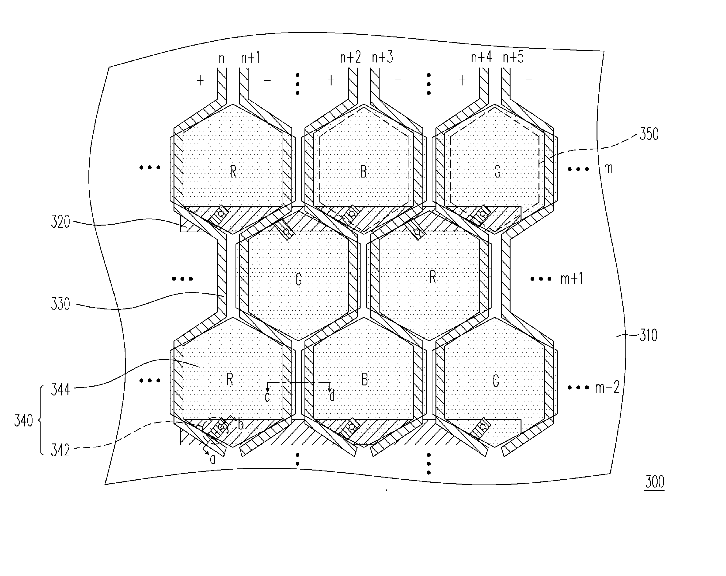
[0038]FIG. 3A is a top view of an active matrix substrate according to the first embodiment of the present invention, and FIGS. 3B and 3C are schematic cross-sectional views along line a-b and line c-d of the active matrix substrate respectively shown in FIG. 3A. Referring to FIGS. 3A through 3C, the active matrix substrate 300 of the present embodiment includes a substrate 310, a plurality of scan lines 320, a plurality of data lines 330 and a plurality of sub-pixels 340. Details of the substrate 310, the scan lines 320, the data lines 330 and the sub-pixels 340 are illustrated below.

[0039] The substrate 310 may be made of glass, quartz or other appropriate materials. The scan lines 320 may be made of aluminum alloy or other appropriate materials. The data lines 330 may be made of chromium alloy, aluminum alloy or other appropriate materials. The scan lines 320 and the data lines 330 are disposed on the substrate 310, and define a plurality of sub-pixel ...

second embodiment

[0047] The Second Embodiment

[0048]FIG. 4A is a top view of an active matrix substrate according to the second embodiment of the present invention. FIGS. 4B and 4C are schematic cross-sectional views along line a-b and line c-d of the active matrix substrate respectively shown in FIG. 4A. Referring to FIGS. 4A through 4C, the active matrix substrate 400 is similar to the active matrix substrate 300 of the first embodiment, and the difference therebetween is that the pixel electrodes 444 of the second embodiment of the invention are configured in a form of rectangular and each of the data lines 430 has multiple turnings incorporating with the shape of the corresponding pixel electrode 444, whereby defining a sub-pixel region 450.

[0049] The advantages of the active matrix substrate 400 according to the second embodiment of the invention are similar with the active matrix substrate 300 according to the first embodiment of the invention, and are not to be repeated.

[0050] Furthermore, i...

third embodiment

[0051] The Third Embodiment

[0052]FIG. 5A is a top view of an active matrix substrate according to the third embodiment of the present invention. FIGS. 5B and 5C are schematic cross-sectional views along line a-b and line c-d of the active matrix substrate respectively shown in FIG. 5A. Referring to FIGS. 5A through 5C, the active matrix substrate 500 is similar to the active matrix substrate 300 of the first embodiment, and the difference therebetween is that according to the third embodiment of the invention, a reference line 544c is defined in each of the pixel electrodes 544, the reference line 544c dividing the pixel electrode 544 into two electrode portions 544a and 544b which are symmetric along the reference line 544c and electrically connected to each other. The two electrode portions 544a and 544b are configured in a form of trapezium. The data line 530 has multiple turnings for incorporating the form of the pixel electrode 544 and therefore defines a shield shaped sub-pixe...


PUM


Abstract

An active matrix substrate including a substrate, a plurality of scan lines, a plurality of data lines and a plurality of sub-pixels is provided. The scan lines and the data lines are disposed on the substrate, and define a plurality of sub-pixel regions distributed in a delta arrangement. The sub-pixels corresponding to the sub-pixel regions are disposed on the substrate. The sub-pixels are electrically connected with corresponding scan lines and corresponding data lines. Between two sub-pixel regions corresponding to any two adjacent sub-pixels at a same side of one scan line, there are two data lines. Each sub-pixel includes an active device and a pixel electrode. The active device is electrically connected with a corresponding scan line and a corresponding data line. The pixel electrode is electrically connected with the active device, and extends from the sub-pixel region corresponding to the sub-pixel to a position over the data line.

Description

CROSS-REFERENCE TO RELATED APPLICATION [0001] This application claims the priority benefit of Taiwan application serial no. 94133945, filed on Sep. 29, 2005. All disclosure of the Taiwan application is incorporated herein by reference. BACKGROUND OF THE INVENTION [0002] 1. Field of the Invention [0003] The present invention relates to an active matrix substrate, and particularly to an active matrix substrate adapted for improving display quality of a liquid crystal display (LCD) using the same. [0004] 2. Description of Related Art [0005] In order to satisfy the modern living, video and image devices are developing towards smaller sizes. Although conventional cathode ray tube (CRT) displays still have some advantages, with respect to the structures of their internal electron cavities, they are too bulky and occupy too much space. They even generate radiation which is harmful to eyes when displaying images. Therefore, flat panel displays such as LCDs, incorporating with new optoelectr...

Claims


Application Information

Patent Timeline
IPC IPC(8): G09G5/02
CPCG02F1/134336G02F2201/52G02F2001/134345G02F1/134345
Inventor LIN, HSIANG-LINLIN, CHING-HUANHUANG, KUO-YU
Owner AU OPTRONICS CORP
Why Eureka
Try Eureka