Supercharge Your Innovation With Domain-Expert AI Agents!

Closed loop controlled reference voltage calibration circuit and method

a reference voltage and calibration circuit technology, applied in the direction of electrical digital data processing, electronic circuit testing, instruments, etc., can solve the problems of not doing calibration at nominal operating conditions, not providing information about level margins about reference voltage, and becoming more difficult to provide a clean signal

Active Publication Date: 2007-03-29
ATI TECH INC
View PDF2 Cites 27 Cited by
  • Summary
  • Abstract
  • Description
  • Claims
  • Application Information

AI Technical Summary

Problems solved by technology

To increase data transfer rates and run interfaces at higher speeds, it becomes more difficult to provide a clean signal and as such the driver strength needs to be controlled to improve signal to noise levels and signal integrity.
However, this method does not do calibration at nominal operating conditions when termination 24 is turned on and non-active transmitter 18 is turned off.
In addition, this method does not provide information about level margins about the reference voltage.
As such, calibration done with the fixed VREF reference voltage provided by the precision resistors that are off-chip, do not allow the detection of how marginal a signal level truly may be.

Method used


Image

  • Closed loop controlled reference voltage calibration circuit and method
  • Closed loop controlled reference voltage calibration circuit and method
  • Closed loop controlled reference voltage calibration circuit and method

Examples


Embodiment Construction

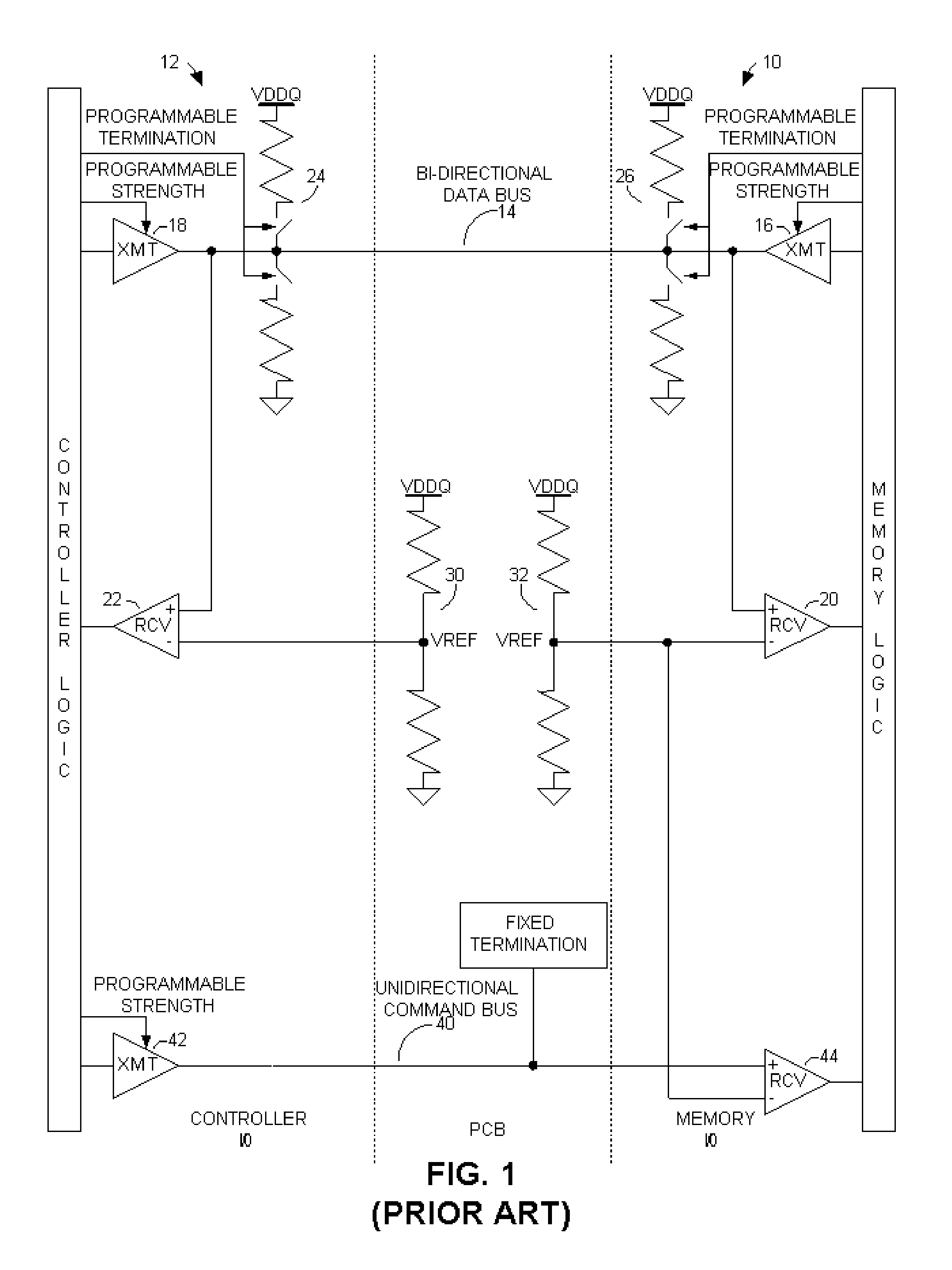
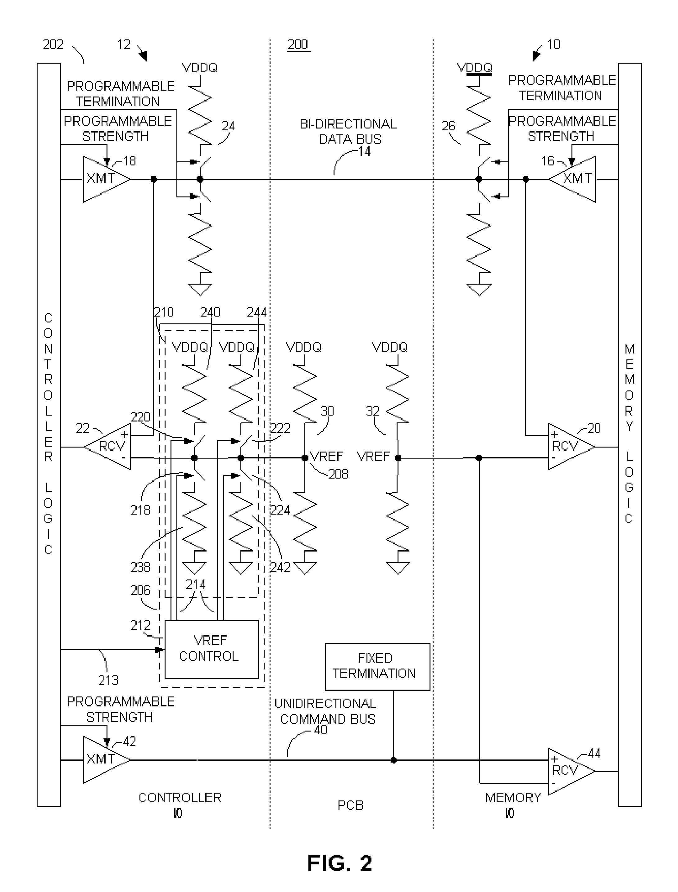
[0018] Briefly, an impedance calibration circuit for an off-chip driver, such as a DDR2 memory driver or any other suitable interface, includes an electronically controllable variable reference voltage circuit that is operatively coupled to a reference voltage, such as an off-chip reference voltage if desired, which varies the reference voltage supplied to a receiver circuit. In one example, the variable reference voltage circuit includes reference voltage control logic and an array of switchable resistor elements consisting of pull-up and pull-down resistor elements that may each be selectively switched on or off to change the reference voltage (VREF) generated by external resistor divider being supplied to, for example, an on-chip receiver.

[0019] A method is also disclosed which includes determining a driver impedance mismatch condition, and varying a reference voltage for a differential receiver circuit by electronically switching at least one of a pull-up resistor element and a...


PUM


Abstract

A variable reference voltage circuit controllable in closed loop, for calibrating off-chip and on-chip drivers, margining and optimizing a reference voltage, for interfaces such as DDR2 or any other suitable interface. In one example, the on-chip variable reference voltage circuit, coupled to external fixed reference voltage, includes control logic and an array of switchable resistor elements (pull-up and pull-down resistors) that may each be selectively switched in or out of the circuit to change the reference voltage being supplied to an on-chip receiver.

Description

FIELD OF THE INVENTION [0001] The invention relates generally to high-speed electrical interface optimization by controlling a closed loop reference voltage of differential receiver to calibrate off-chip and on-chip driver strength (impedance), and margin and optimize a reference voltage for reliable data transfer. BACKGROUND OF THE INVENTION [0002] High-speed interfaces and associated transmitters and corresponding differential receivers suitable for high-speed data transfers are known. High speed requires precisely adjusted transmitters and receivers to provide reliable data transfer. To increase data transfer rates and run interfaces at higher speeds, it becomes more difficult to provide a clean signal and as such the driver strength needs to be controlled to improve signal to noise levels and signal integrity. For example, a double data rate (DDR2) memory interface has a type of Off-Chip Driver calibration mechanism (OCD—Off-Chip Driver calibration) to allow for a transmitter on...

Claims


Application Information

Patent Timeline
Patent Type & Authority Applications(United States)
IPC IPC(8): G01R35/00G06F19/00
CPCG01R31/30G01R31/3004G01R31/3173G11C29/028G11C29/02G11C29/021G11C5/147
Inventor BOSKOVIC, BORIS
Owner ATI TECH INC
Features
  • R&D
  • Intellectual Property
  • Life Sciences
  • Materials
  • Tech Scout
  • Unparalleled Data Quality
  • Higher Quality Content
  • 60% Fewer Hallucinations
Learn More