Process for producing wiring circuit board
Inactive Publication Date: 2007-04-05
NITTO DENKO CORP
View PDF6 Cites 6 Cited by
- Summary
- Abstract
- Description
- Claims
- Application Information
AI Technical Summary
Benefits of technology
[0023] By regulating the temperature in the heat treatment on the conductor pattern and tin film to 175 to 225° C. and the time period of this heat treatment to 2 to 10 minutes, the tin film can be made to retain a necessary thickness after the heat curing treatment of the solder resist and the increase in mixture layer thickness through this heat curing treatment can be reduced. As a result, the unevenness of the connectivity of the conductor pattern with electronic parts can be reduced while securing the connectivity.
[0024] (3) The temperature in the heat curing treatment on the solder resist may be 80 to 160° C. In this case, the tin film can retain a necessary thickness without fail after the heat curing treatment on the solder resist and the increase in mixture layer thicknes
Problems solved by technology
However, in the wiring circuit board produced by the above-described method, the unevenness of connectivity with electronic parts becomes high.
This results in considerable fluctuations in product yield.
As a result, it is found that the mixture layer of copper and tin formed by
Method used
View moreImage
Smart ImageViewing Examples

Examples
example 1
[0091] The heat treatment temperature was regulated to 175° C. and the heat treatment period was regulated to each of 2 minutes, 5 minutes, and 10 minutes.
example 2
[0092] The heat treatment temperature was regulated to 185° C. and the heat treatment period was regulated to each of 2 minutes, 5 minutes, and 10 minutes.
example 3
[0093] The heat treatment temperature was regulated to 200° C. and the heat treatment period was regulated to each of 2 minutes, 5 minutes, and 10 minutes.
Login to view more PUM
 Abstract
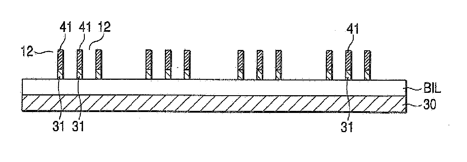
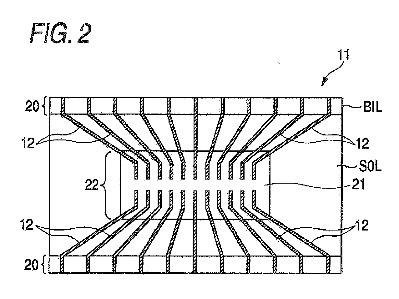
The present invention provides a process for producing a wiring circuit board which can be inhibited from developing whiskers and can be reduced in the unevenness of connectivity with electronic parts while retaining the connectivity. According to the present invention, a wiring pattern 12 comprising a thin metal film 31 and a conductor layer 33 is formed on a base insulating layer BIL. A tin-plated layer 34 is formed by electroless plating so as to coat the wiring pattern 12 therewith. The wiring pattern 12 and the tin-plated layer 34 are then subjected to a heat treatment. The heat treatment temperature and heat treatment period are regulated to 175 to 225° C. and 2 to 10 minutes, respectively. By the heat treatment, a mixture layer 35 comprising copper and tin is formed. Thereafter, a solder resist SOL is formed over the base insulating layer so as to cover the wiring pattern 12 and tin-plated layer 34 in given regions. Subsequently, the solder resist SOL is subjected to a heat curing treatment.
Description
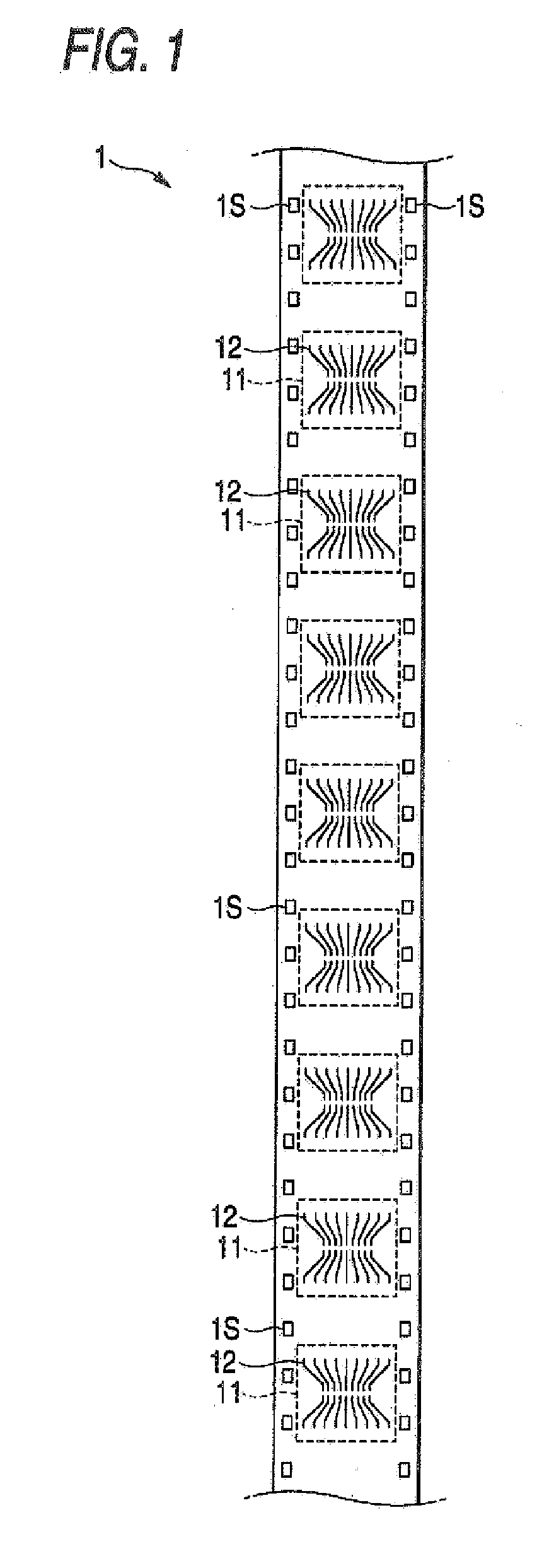
FIELD OF THE INVENTION [0001] The present invention relates to a process for producing a wiring circuit board. BACKGROUND OF THE INVENTION [0002] Wiring circuit boards such as TAB (tape automated bonding) tape carrier generally contain a substrate containing an insulating layer and, formed thereon, a wiring pattern containing a conductor layer, and are used in various electronic appliances. [0003] Various electronic parts are mounted on a wiring circuit board and connected to terminal parts of the wiring pattern. The terminals of the electronic parts are made of, e.g., gold. In this case, in order to improve the connectivity of the terminal parts of the wiring pattern with the terminals of such electronic parts, a tin film (tin deposit) is formed so as to coat the terminal parts of the wiring pattern therewith. Herein, the term “connectivity of wiring pattern with electronic part” means the certainty of electrical and physical connection between the wiring pattern and the electronic...
Claims
Login to view more Application Information
Patent Timeline
 IPC IPC(8): H01L21/44
CPCH05K3/06H05K3/108H05K3/244H05K3/28H05K2203/1105H05K3/00
Inventor TSUNEKAWA, MAKOTO
Owner NITTO DENKO CORP
- R&D Engineer
- R&D Manager
- IP Professional
Why Eureka
- Industry Leading Data Capabilities
- Powerful AI technology
- Patent DNA Extraction
Try Eureka
Browse by: Latest US Patents, China's latest patents, Technical Efficacy Thesaurus, Application Domain, Technology Topic.
© 2024 PatSnap. All rights reserved.Legal|Privacy policy|Modern Slavery Act Transparency Statement|Sitemap