Supercharge Your Innovation With Domain-Expert AI Agents!

Wafer edge exposure method in semiconductor photolithographic processes, and orientation flatness detecting system provided with a WEE apparatus

a technology of semiconductor photolithography and edge exposure, which is applied in the field of semiconductor photolithographic processes, can solve the problems of unnecessarily long total processing time in the stepper and the decrease of the yield of semiconductor devices on the wafer, and achieve the effect of reducing the total processing time of photolithographic processing

Inactive Publication Date: 2007-04-19
DONGBU ELECTRONICS CO LTD
View PDF5 Cites 7 Cited by
  • Summary
  • Abstract
  • Description
  • Claims
  • Application Information

AI Technical Summary

Benefits of technology

[0008] It is therefore an object of the present invention to provide a method for exposing an edge of a semiconductor wafer in a photolithographic process that enables reduction of the total processing time in photolithographic processing.
[0009] Another object of the present invention is to provide an OF detecting system with a WEE apparatus, which can facilitate photolithographic processing according to the present method.

Problems solved by technology

If the portion of the photoresist peels off, the yield of semiconductor devices from the wafer may decrease.
As a result, a waiting time in the OF detecting system may increase so that the total processing time in the stepper may be unnecessarily long.

Method used


Image

  • Wafer edge exposure method in semiconductor photolithographic processes, and orientation flatness detecting system provided with a WEE apparatus
  • Wafer edge exposure method in semiconductor photolithographic processes, and orientation flatness detecting system provided with a WEE apparatus
  • Wafer edge exposure method in semiconductor photolithographic processes, and orientation flatness detecting system provided with a WEE apparatus

Examples


Embodiment Construction

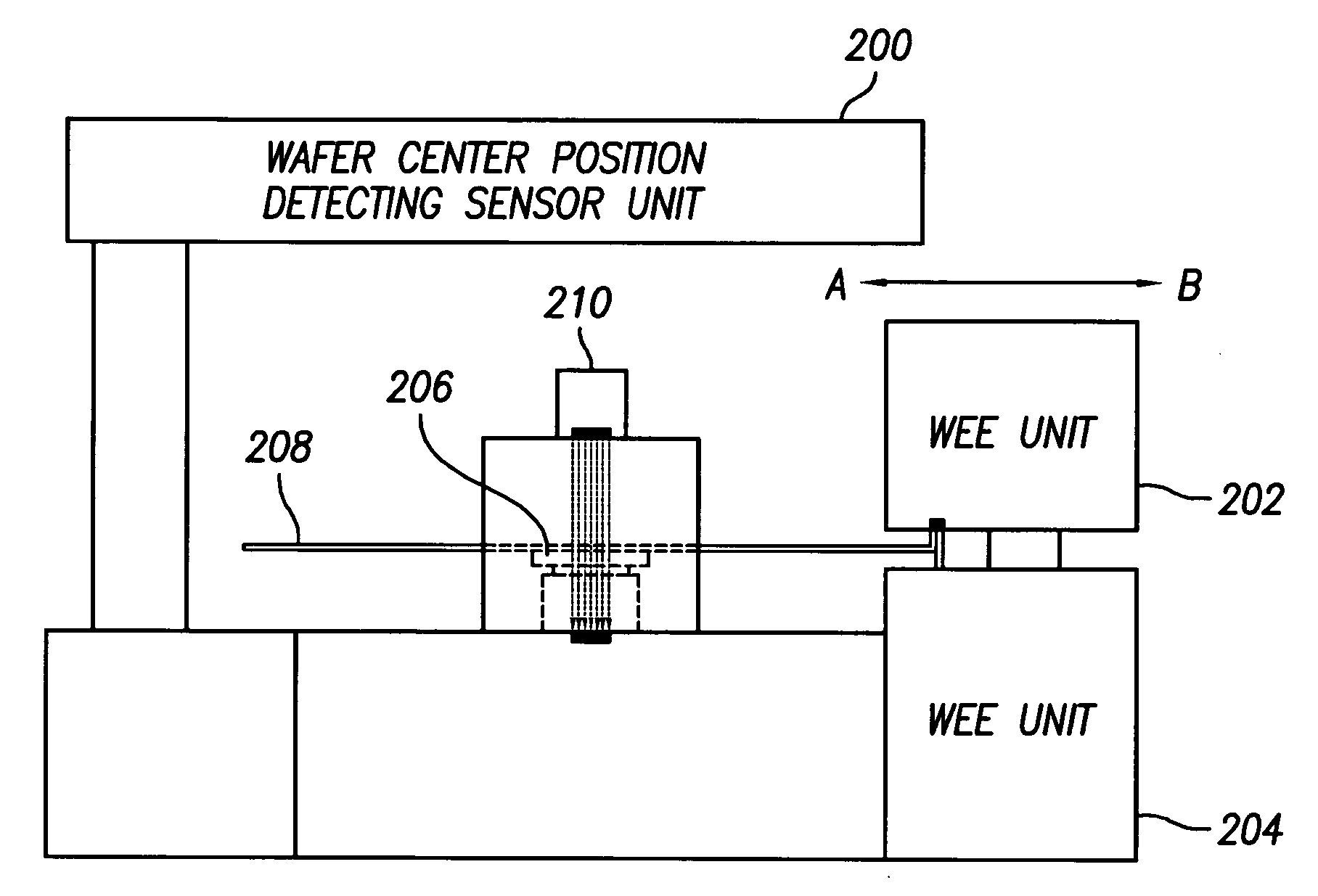
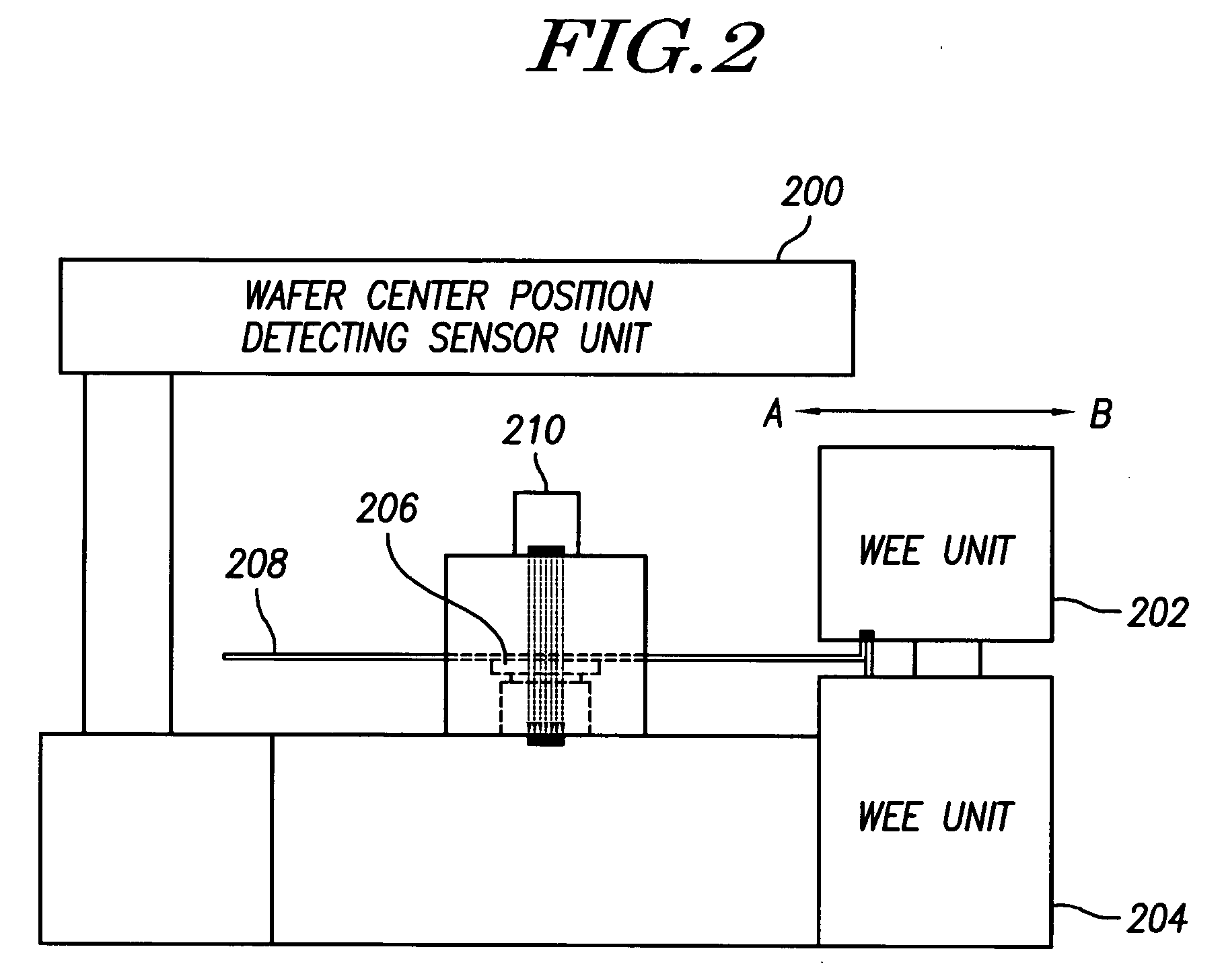
[0017]FIG. 2 shows a cross-sectional view of an OF detecting system further including a WEE apparatus according to an embodiment of the present invention. Referring to FIG. 2, the OF (Orientation Flatness) detecting system comprises a wafer notch detecting sensor unit 210 adapted (or configured) to detect a notch of a wafer 208, a wafer center position detecting sensor unit 200 adapted (or configured) to detect the center of the wafer 208, a WEE (Wafer Edge Exposure) unit 202 adapted (or configured) to perform a WEE process, a WEE driving unit 204 adapted (or configured) to change a position of the WEE unit 202, and a wafer chuck 206.

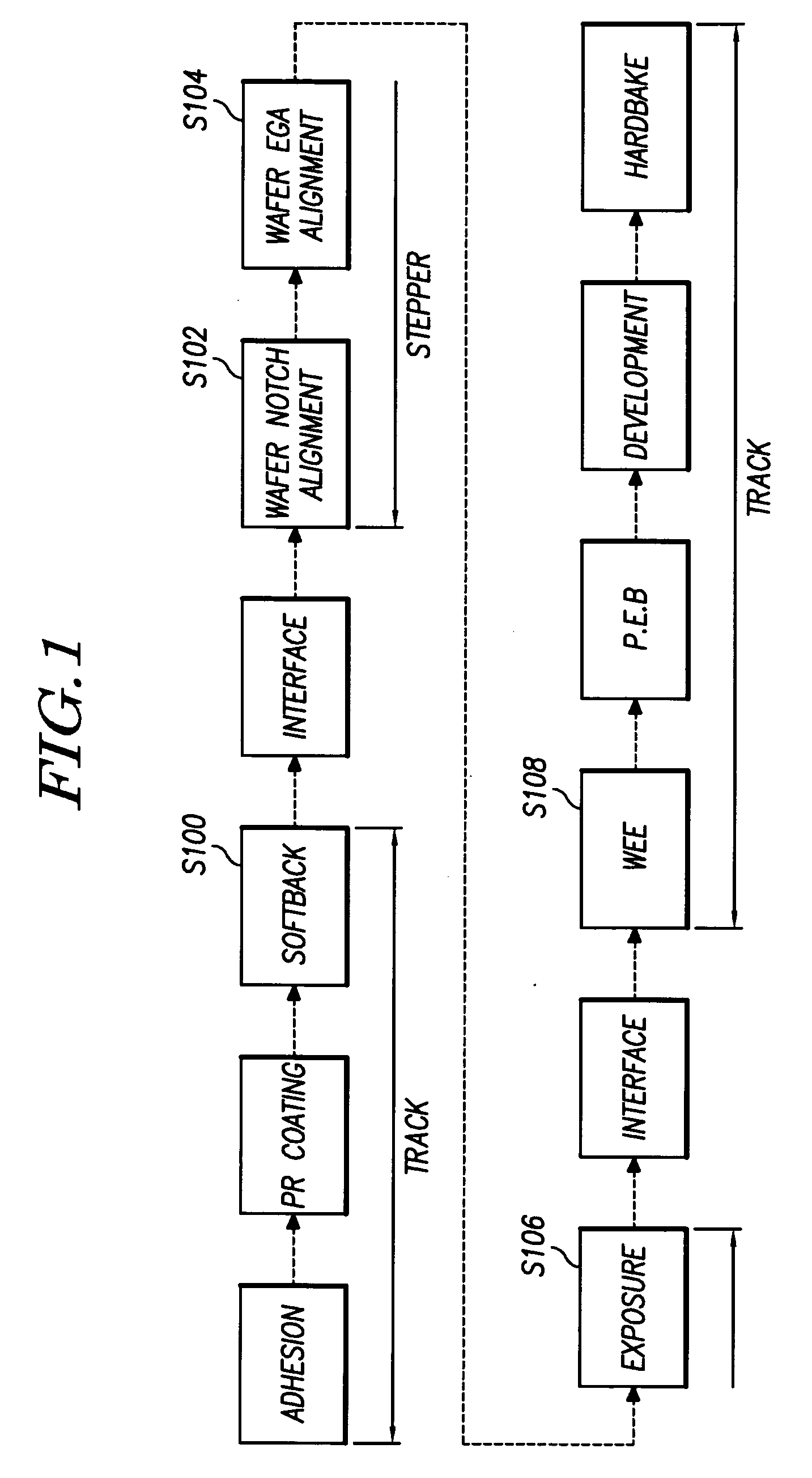
[0018]FIG. 3 shows a series of photolithographic processes using the OF detecting system provided with a WEE apparatus according to the present invention. Hereinafter, the preferred embodiment of the present invention will be explained in detail with reference to FIGS. 2 and 3.

[0019] First, after the wafer 208 is coated with a photoresist and soft bak...


PUM


Abstract

The present invention relates to a method for exposing an edge of a semiconductor wafer in photolithographic processes, and an OF (Orientation Flatness) detecting system provided with a WEE (Wafer Edge Exposure) apparatus. According to the present invention, a notch-aligned wafer can be treated by a WEE process on a wafer chuck of an OF detecting system, without waiting for its patterning exposure process to be performed first. Thus, the total processing time in photolithographic processes can be decreased.

Description

BACKGROUND OF THE INVENTION [0001] 1. Field of the Invention [0002] The present invention relates to semiconductor photolithographic processes. More specifically, the present invention relates to a method for exposing an edge of a semiconductor wafer in photolithographic processes, and an OF (Orientation Flatness) detecting system provided with a WEE (Wafer Edge Exposure) apparatus. [0003] 2. Description of the Related Art [0004] Conventionally, a wafer edge exposure (WEE) process additionally exposes a round edge and ID region of a wafer after exposing the wafer provided with a photoresist in a stepper. In such a wafer edge exposure process, a portion of the photoresist formed on the edge of the wafer is removed. This prevents the portion of the photoresist on the edge from peeling off during photolithographic processes. If the portion of the photoresist peels off, the yield of semiconductor devices from the wafer may decrease. [0005]FIG. 1 shows a series of conventional photolitho...

Claims


Application Information

Patent Timeline
Patent Type & Authority Applications(United States)
IPC IPC(8): G03B27/42
CPCG03F7/2028G03F7/70425H01L21/682
Inventor KIM, OOK HYUN
Owner DONGBU ELECTRONICS CO LTD
Features
  • R&D
  • Intellectual Property
  • Life Sciences
  • Materials
  • Tech Scout
  • Unparalleled Data Quality
  • Higher Quality Content
  • 60% Fewer Hallucinations
Learn More