Method for forming improved bump structure

a bump structure and bump technology, applied in the field of flip chip packaging technology, can solve the problems of reducing circuit resistance, affecting electrical performance, and low potential failure point, and achieve the effect of improving the bump structur

Inactive Publication Date: 2007-04-19
TAIWAN SEMICON MFG CO LTD
View PDF3 Cites 52 Cited by
  • Summary
  • Abstract
  • Description
  • Claims
  • Application Information

AI Technical Summary

Problems solved by technology

Packages with fewer interconnecting links lower potential failure points, reduce the circuit resistance, and reduce interconnect capacitance, which affects electrical performance.
One recurring problem with the prior art method of forming solder bump structures is that frequently, delaminations occur in the UBM layers.

Method used


Image

  • Method for forming improved bump structure
  • Method for forming improved bump structure
  • Method for forming improved bump structure

Examples


Embodiment Construction

[0014] In the following description, numerous specific details are set forth to provide a thorough understanding of the present invention. However, one having an ordinary skill in the art will recognize that the invention can be practiced without these specific details. In some instances, well-known structures and processes have not been described in detail to avoid unnecessarily obscuring the present invention.

[0015] Reference will now be made in detail to the present preferred embodiments of the present invention, examples of which are illustrated in the accompanying drawings.

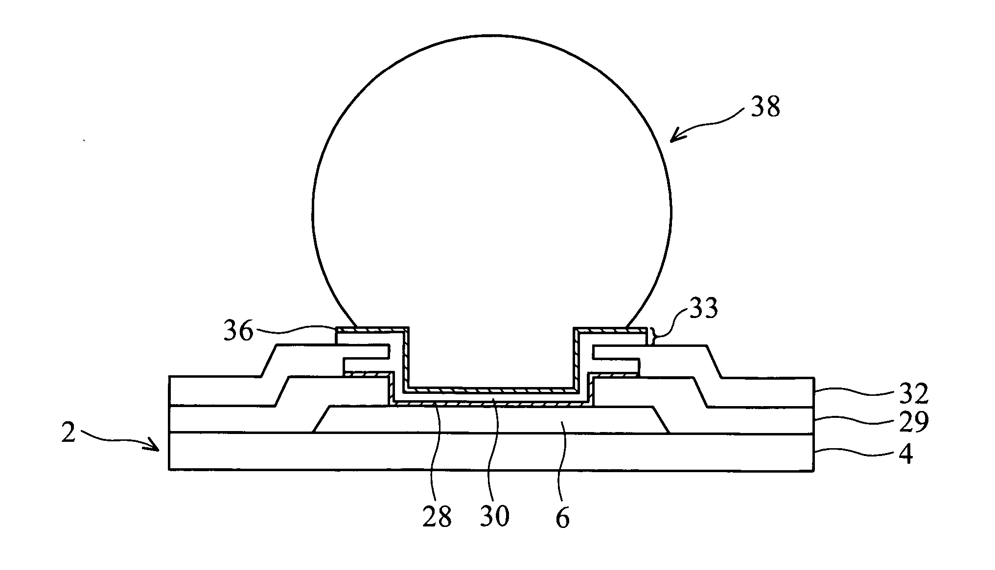
[0016] As shown in FIG. 2A, a cross-sectional view of a semiconductor device depicting a method of forming a solder bump structure according to one embodiment of the present invention is provided. A semiconductor wafer 2 is provided having a base semiconductor substrate 4 with metal interconnect layers (not shown) overlying substrate 4 and a first passivation layer 29, which may be one or more layers, that ...


PUM


Abstract

Methods for forming an improved bump structure on a semiconductor device are provided. In one embodiment, a substrate is provided having at least one contact pad formed thereon. A first passivation layer is formed over the substrate, the first passivation layer having at least one opening therein exposing a portion of the contact pad. A first patterned and etched conductive metal layer is formed on the contact pad and above a portion of the first passivation layer. A second patterned and etched passivation layer is formed above the first passivation layer and a portion of the first conductive metal layer, wherein a portion of the ends of the first conductive metal layer is wedged between the first and second passivation layers. A second conductive metal layer is formed above the second passivation layer and the first conductive metal layer. A patterned and etched photoresist layer is then formed over a portion of the second passivation layer, the photoresist layer having an opening overlying the contact pad, and a solder material is deposited in the opening to form a solder column. The photoresist layer is thereafter removed and the second conductive metal layer is etched to the second passivation layer by using the solder column as an etching mask. The solder column is then reflown to create a solder bump.

Description

BACKGROUND OF THE INVENTION [0001] 1. Field of the Invention [0002] The present invention relates generally to flip chip packaging technology, and more particularly, to methods for forming improved bump structures. [0003] 2. Description of the Related Art [0004] Faster, reliable, and higher-density circuits at lower costs are the goals for integrated circuit (IC) packaging. Conventional wirebond technology, the most common method for electrically connecting aluminum bonding pads on a chip surface to the package inner lead terminals on the lead-frame or substrate has proven to be low cost and reliable. But for the future, packaging goals will be met by increasing the density of chips and reducing the number of internal interconnections. Packages with fewer interconnecting links lower potential failure points, reduce the circuit resistance, and reduce interconnect capacitance, which affects electrical performance. The need to reduce the IC package to fit end-user applications (e.g., S...

Claims


Application Information

Patent Timeline
Patent Type & Authority Applications(United States)
IPC IPC(8): H01L21/44
CPCH01L24/03H01L23/3192H01L24/11H01L24/12H01L2224/03912H01L2224/0401H01L2224/05022H01L2224/05558H01L2224/05567H01L2224/05624H01L2224/05647H01L2224/1132H01L2224/1147H01L2224/13007H01L2224/13022H01L2224/131H01L2924/01013H01L2924/01014H01L2924/01022H01L2924/01028H01L2924/01029H01L2924/0105H01L2924/01078H01L2924/01082H01L2924/014H01L2924/05042H01L2924/14H01L2924/30105H01L24/05H01L2224/05018H01L2224/0558H01L2924/0002H01L2924/01033H01L2924/00013H01L2924/00014H01L2224/13099H01L2224/05552
Inventor CHANG, HSU-LIANGCHU, CHING-HUA
Owner TAIWAN SEMICON MFG CO LTD
Why Eureka
Try Eureka