
Light-emitting element having at least one light-emitting chip crystal

a technology of light-emitting chips and light-emitting elements, which is applied in the direction of semiconductor devices for light sources, semiconductor/solid-state device details, lighting and heating apparatus, etc., can solve the problems of limited supply voltage and therefore emission outpu

Inactive Publication Date: 2007-04-26
NOCTRON
View PDF7 Cites 33 Cited by
  • Summary
  • Abstract
  • Description
  • Claims
  • Application Information

AI Technical Summary

Benefits of technology

[0007] According to one aspect of the present invention, a fluid surrounds the light-emitting chip crystal, insulates it in this way mechanically, chemically, and / or electrically from air and the environment and removes the heat which arises. By the fact that the fluid is in direct contact, which in particular is free from air or gas bubbles, with the light-emitting chip crystal, the heat which arises when the light-emitting chip crystal is charged with the supply voltage is transferred to the fluid and transported away with this, so that the light-emitting chip crystal is cooled.
[0008] As a result, premature overheating of the fluid is also prevented, so that this also does not change optically in particular and in the worst case “die.” In this manner, the light-emitting chip crystal can be operated at a significantly higher supply voltage than is possible when transparent resin is used.
[0009] Cooling of the light-emitting chip crystal furthermore has the effect of a significant improvement in its efficiency in respect of emission. Overall, an increase in the emission output is thus achieved due to a higher maximum supply voltage and / or the improvement in the efficiency, even at a low supply voltage.

Problems solved by technology

In the case of known light-emitting elements, the supply voltage and therefore the emission output are limited in particular by the heat resistance of the transparent resin.

Method used


Image

  • Light-emitting element having at least one light-emitting chip crystal
  • Light-emitting element having at least one light-emitting chip crystal
  • Light-emitting element having at least one light-emitting chip crystal

Examples


Embodiment Construction

[0040] While this invention is susceptible of embodiment in many different forms, there is shown in the drawings and will herein be described in detail one or more embodiments with the understanding that the present disclosure is to be considered as an exemplification of the principles of the invention and is not intended to limit the invention to the embodiments illustrated.

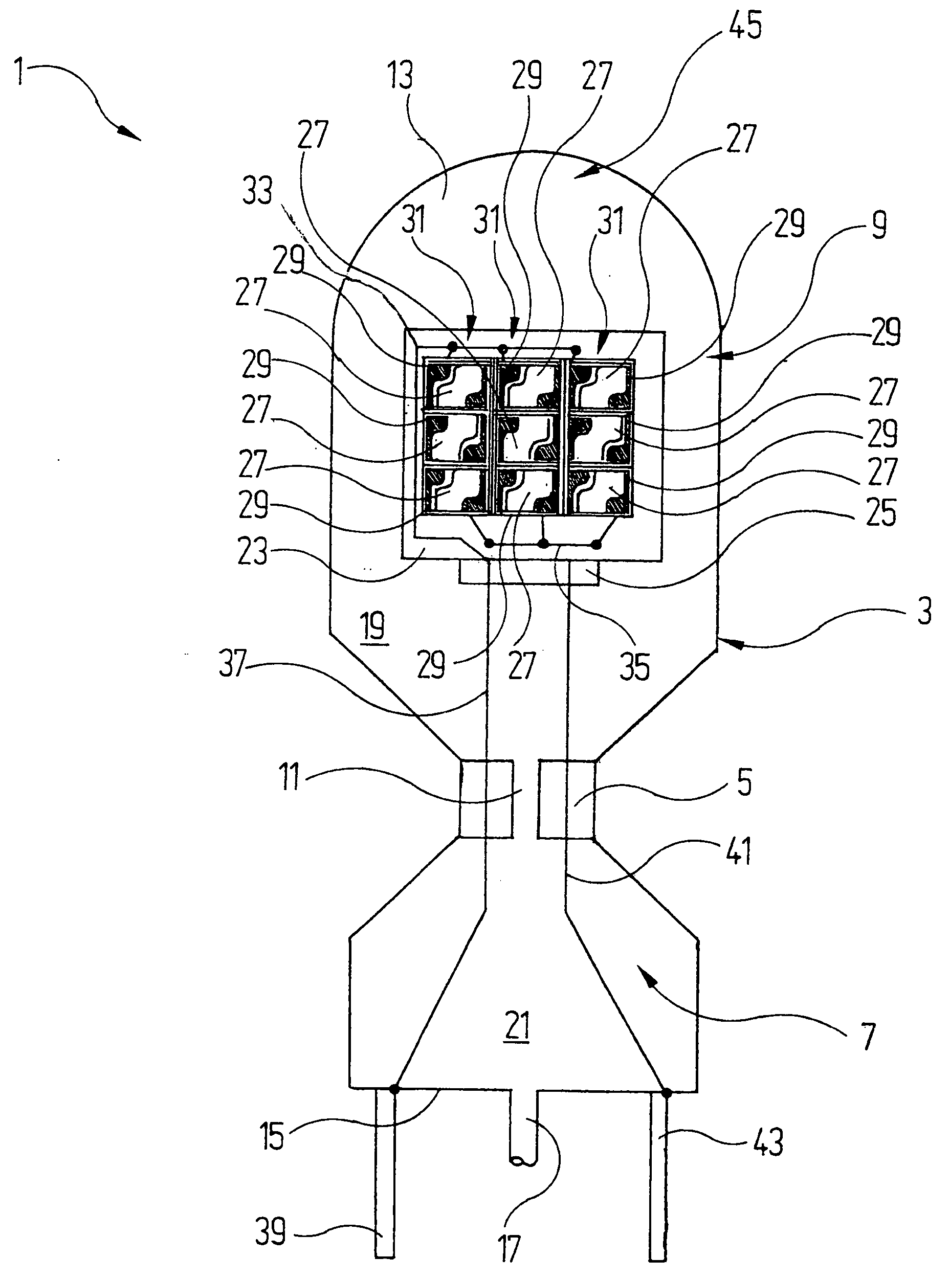
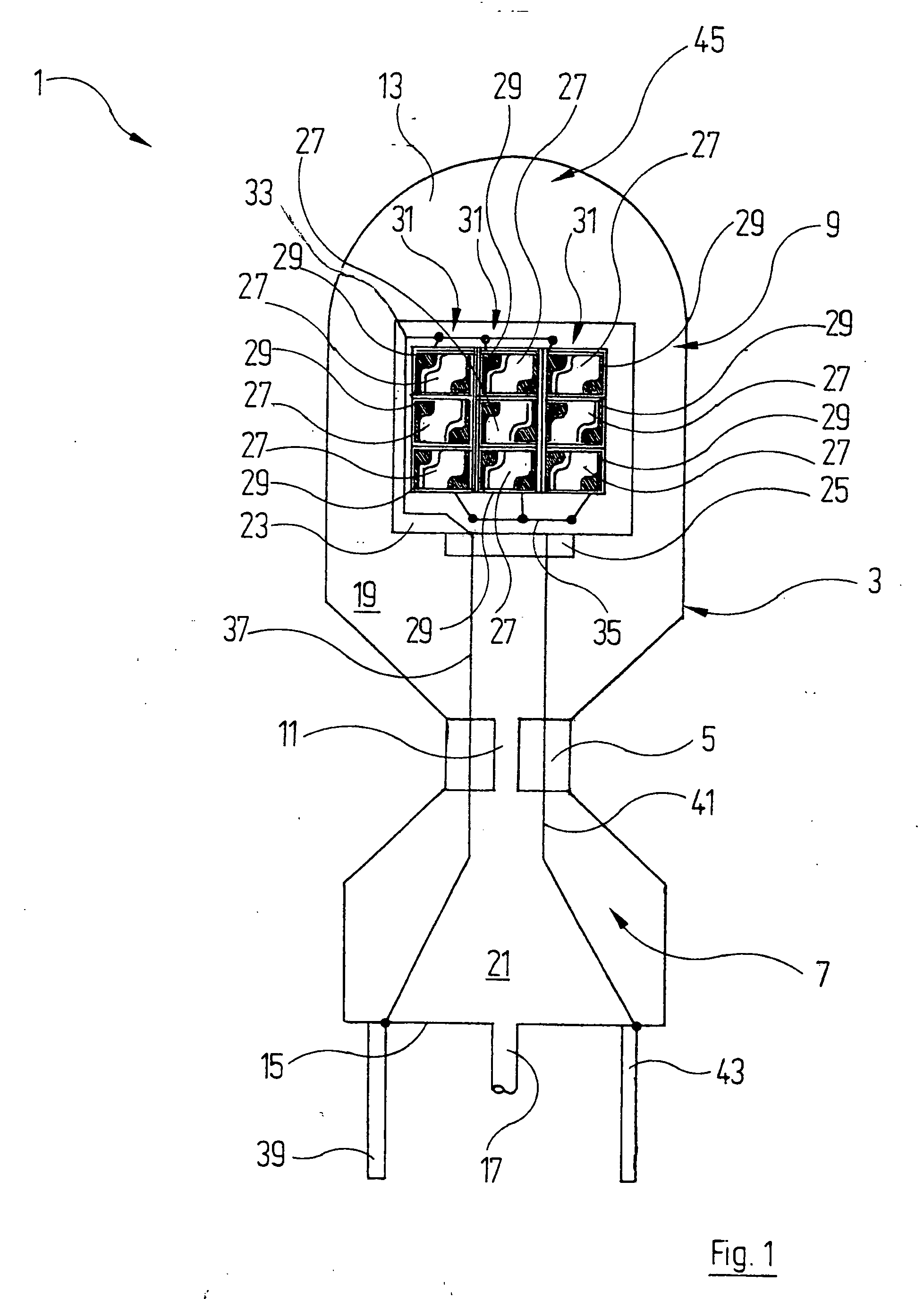
[0041] A light-emitting diode given overall the reference symbol 1 is shown in FIG. 1. The light-emitting diode 1 has a hollow cylindrical housing 3 of glass which is transparent to light, the axis thereof running vertically in FIG. 1.

[0042] The housing 3 is divided via a horizontal dividing wall 5 in a narrowing of the housing 3 into a pre-chamber 7, at the bottom in FIG. 1, and a main chamber 9, at the top in FIG. 1.

[0043] Centrally in the dividing wall 5 is a through-channel 11 running vertically, via which the pre-chamber 7 is connected to the main chamber 9.

[0044] The upper face of the housing 3 is sphe...


PUM


Abstract

A light-emitting element, in particular a light-emitting diode, having at least one light-emitting chip crystal, in particular a semiconductor crystal, is described. At least free surfaces of the light-emitting chip crystal are covered with an inert material—liquid fluid—which is in direct contact with the light-emitting chip crystal.

Description

RELATED APPLICATIONS [0001] The present invention claims the benefit of the filing date of German Patent Application, Serial No. 10 2005 050 947.9, filed Oct. 22, 2005; the content of which is incorporated by reference herein. TECHNICAL FIELD [0002] The invention relates to a light-emitting element, in particular a light-emitting element similar to a light-emitting diode, having at least one light-emitting chip crystal, in particular a semiconductor crystal, wherein at least one free surface of the light-emitting chip crystal is covered with an inert material. BACKGROUND OF THE INVENTION [0003] Known light-emitting elements, in particular light-emitting diodes, comprise light-emitting chip crystals of semiconductor structures, with which light is emitted in a characteristic wavelength for the semiconductor structures or a characteristic wavelength range. [0004] The light-emitting chip crystals are arranged on substrates and are cast in a transparent resin together with these. The li...

Claims


Application Information

Patent Timeline
Patent Type & Authority Applications(United States)
IPC IPC(8): H01L33/00H01L33/54
CPCF21K9/00F21V29/58H01L2224/48137H01L33/54F21Y2115/10
Inventor DIAMANTIDIS, GEORG
Owner NOCTRON
Learn More