Image sensor package structure

a technology of image sensor and package structure, applied in the direction of basic electric elements, electrical equipment, semiconductor devices, etc., can solve the problems of poor product yield, difficult control of glue, and yield loss, and achieve the effect of improving the package yield of image sensor

Inactive Publication Date: 2007-04-26
SIGURD MICROELECTRONICS CORP
View PDF12 Cites 12 Cited by
  • Summary
  • Abstract
  • Description
  • Claims
  • Application Information

AI Technical Summary

Benefits of technology

[0008] An object of the present invention is to provide an image sensor package structure, which is a CMOS image sensor (CIS) package structure. The present invention can prevent the glue layer from contaminating the solder balls and the sensing region under the trend toward to compactness of image sensor, and can also greatly enhance the package yield of image sensor.

Problems solved by technology

For the above structure, the control of glue is difficult due to slight fluidity of glue when forming the glue layer 17.
When the solder balls 14 undergo the SMT IR reflow process afterward, there will be yield loss.
Moreover, the above two situations will deteriorate with the trend toward compactness of multimedia products and the shrinkage of distance between the pads 20 and the solder balls 14, hence badly affecting the process cost and the product yield.

Method used


Image

  • Image sensor package structure
  • Image sensor package structure
  • Image sensor package structure

Examples


Embodiment Construction

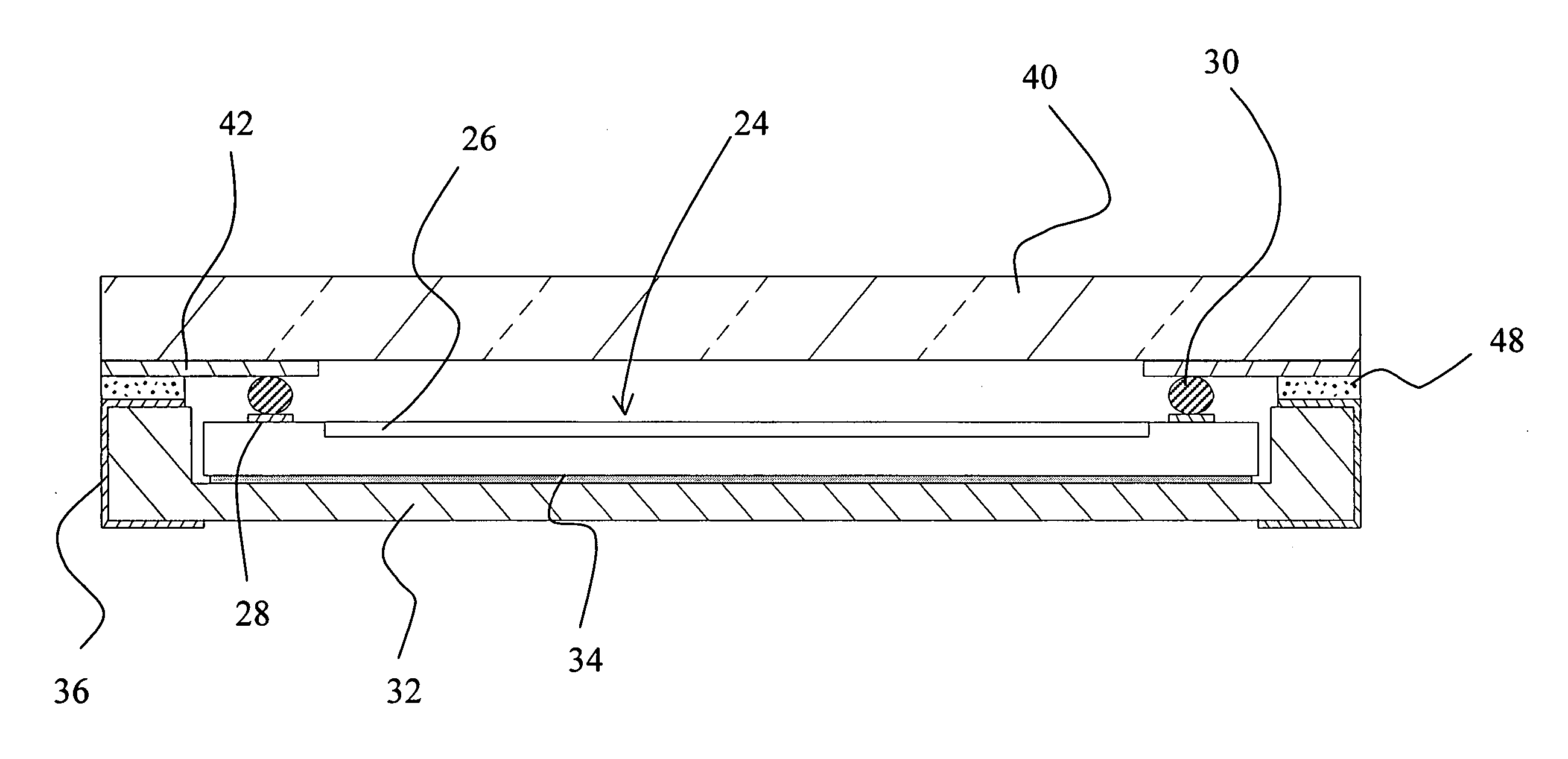
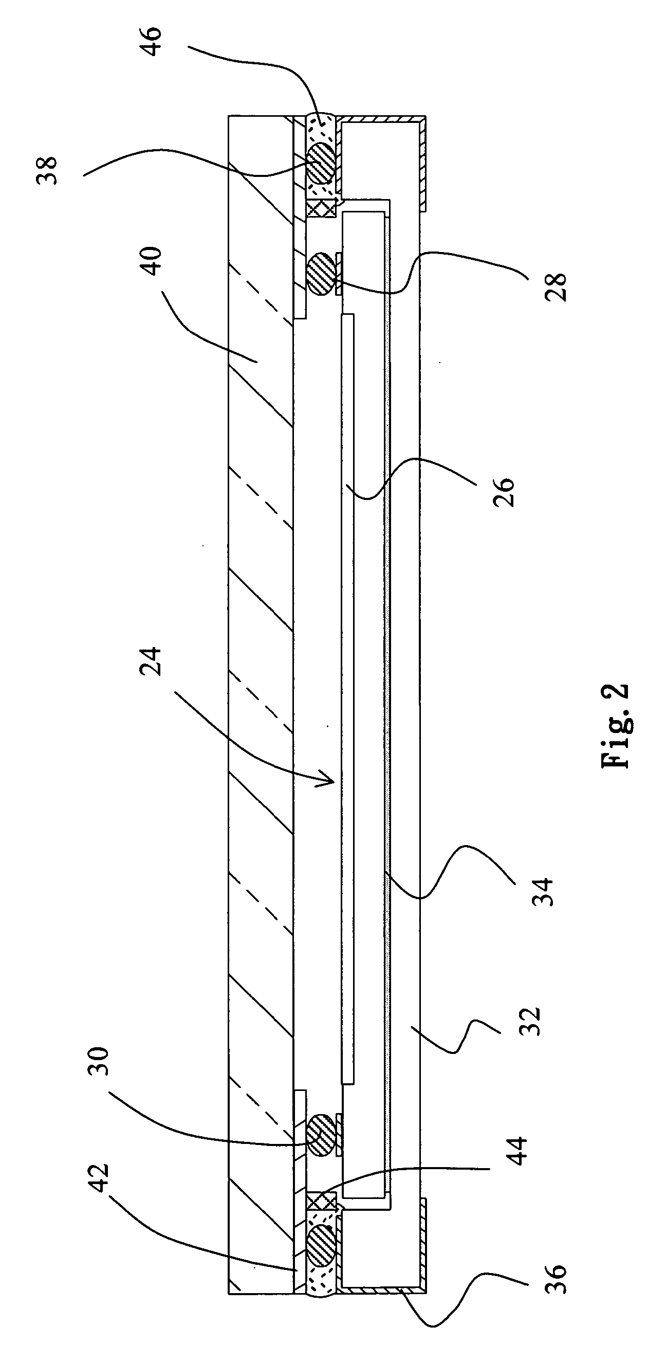
[0019]FIG. 2 is a diagram of an image sensor package structure according to an embodiment of the present invention. The image sensor package structure comprises an image sensor 24, a substrate 32, a light transparent layer 40, a spacer 44, and a glue layer 46. The image sensor 24 includes a sensing region 26 and several pads 28. The pads 28 have several metal connection points 30. An adhesion layer 34 adhere the image sensor 24 to the substrate 32. A metallization trace 36 is disposed at the surface of the substrate 32. Several metal connection points 38 are provided on the metallization trace 36. The light transparent layer 40 covers the image sensor 24 and the substrate 32. The light transparent layer 40 can be a light transparent glass capable of filtering out a certain light wavelength. A metallization trace 42 is disposed on the light transparent layer 40. The metal connection points 30, the metallization trace 42, the metal connection points 38, and the metallization trace 36 ...


PUM


Abstract

An image sensor package structure is proposed, in which an image sensor is fixed on a substrate having metallization traces and an adhesion layer. Electric paths of the package structure are changed from the COG (chip on glass) process to the CIS (CMOS image sensor) process to improve electric characteristics. Moreover, spacers are formed at appropriate positions to prevent glue overflow from contaminating the sensing regions and solder balls. The proposed package structure can also shrink the package area to greatly enhance the yield and quality.

Description

BACKGROUND OF THE INVENTION [0001] 1. Field of the Invention [0002] The present invention relates to an image sensor package structure and, more particularly, to a CMOS image sensor (CIS) package structure. [0003] 2. Description of Related Art [0004] Along with the popularity of audio-video multimedia, image digitization has become an inevitable trend. In recent years, products like digital still cameras (DSCs), digital video camcorders, and image scanners have been continually presented to the public, representing the advent of the era of image digitization. The CMOS technology is a very important technique in this digital era. The advantage and disadvantage, cost, humanized design of CMOS products are keys to success in fierce competitions for enterprises in this field. [0005]FIG. 1 is a diagram of a chip-on-glass (COG) package structure of a conventional CMOS image sensor. The COG package structure comprises a light transparent substrate 10, an image sensor 16, and a glue layer 1...

Claims


Application Information

Patent Timeline
Patent Type & Authority Applications(United States)
IPC IPC(8): H01L31/0203
CPCH01L27/14618H01L27/14683H01L31/0203H01L2924/0002H01L2924/00
Inventor CHEN, PO-HUNGCHEN, MAO-JUNG
Owner SIGURD MICROELECTRONICS CORP
Why Eureka
Try Eureka