Wide window clock scheme for loading output FIFO registers

Active Publication Date: 2007-04-26
PROMOS TECH INC
View PDF2 Cites 6 Cited by
  • Summary
  • Abstract
  • Description
  • Claims
  • Application Information

AI Technical Summary

Benefits of technology

[0013] According to an embodiment of the present invention, a circuit and method provides the widest possible window for capturing data and preventing run-through in a FIFO. The circuit of the present invention is designed to fail when the data-path of the chip is too slow to match the given clock rate. The overall performance is thus limited by the integrated circuit memory itself and not the FIFO loading scheme.

Problems solved by technology

The overall performance is thus limited by the integrated circuit memory itself and not the FIFO loading scheme.

Method used


Image

  • Wide window clock scheme for loading output FIFO registers
  • Wide window clock scheme for loading output FIFO registers
  • Wide window clock scheme for loading output FIFO registers

Examples


Embodiment Construction

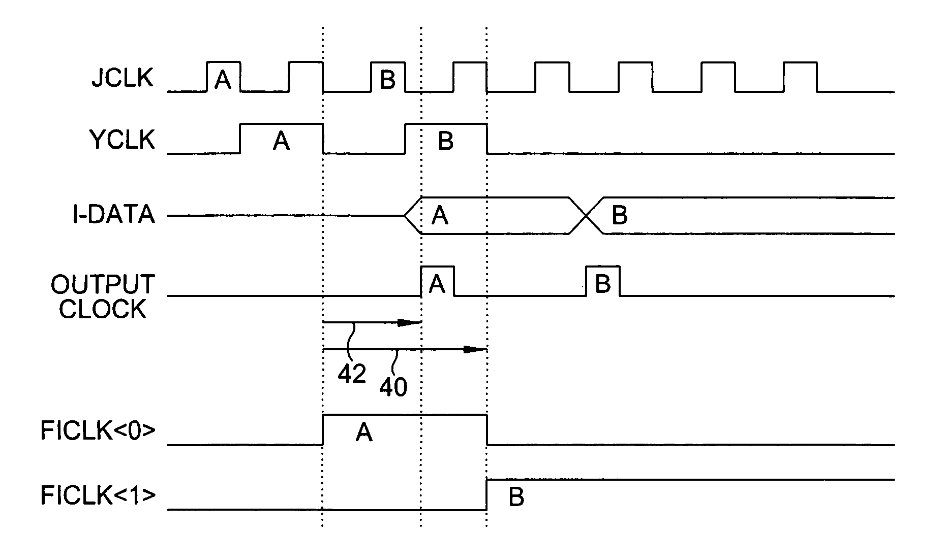
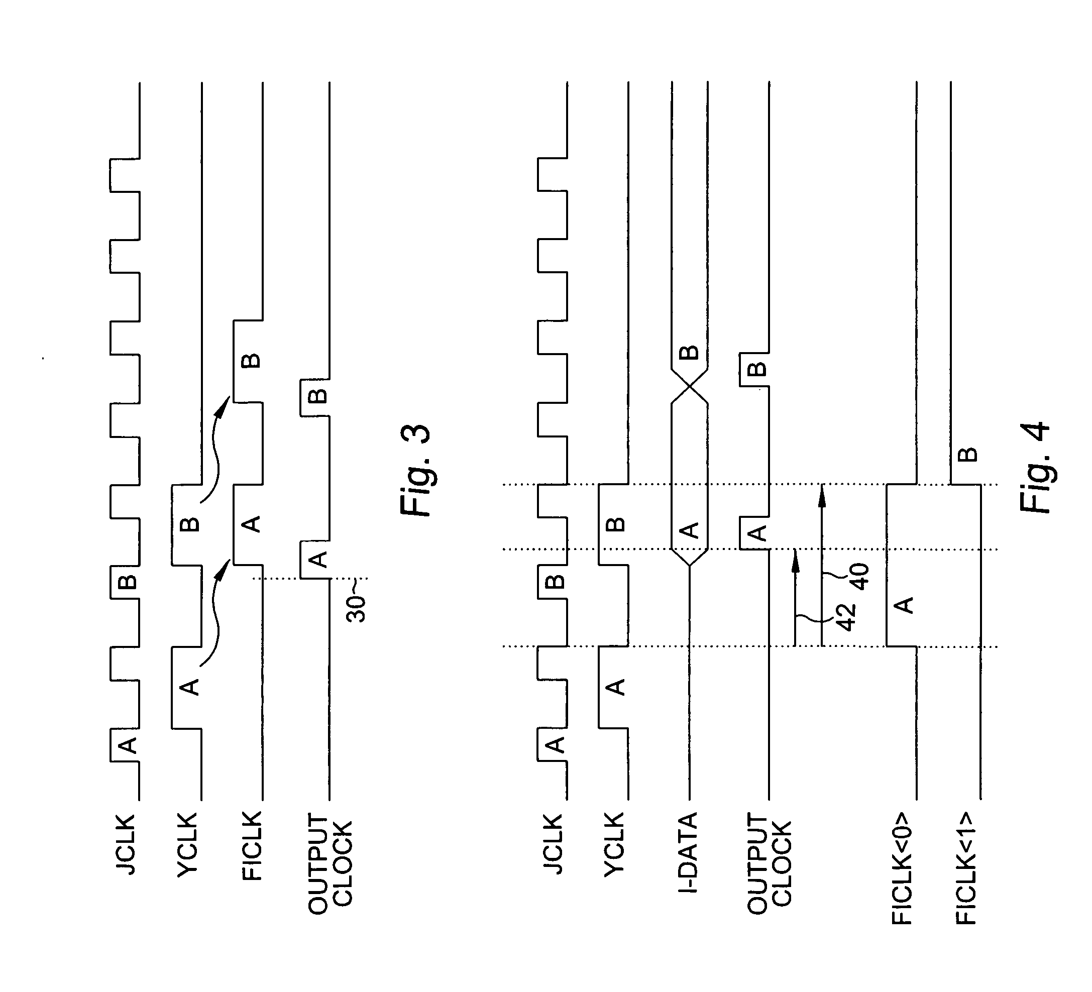
[0029] According to the present invention, a FICLK is enabled, but not activated, based on information from the external clock. In this way, the FIFO is always loaded with the correct data, prior to its being output from the chip. The number of clock edges after the external read command is given before the FICLK is enabled is a function of the desired CL (CAS Latency). The FICLK is fully activated when the previous FICLK is disabled.

[0030] The previous FICLK is disabled only based upon information from the YCLK. Under the DDR2 standard, data only shows up in our datapath on the falling edge of a YCLK, so therefore that event is chosen as the defining point for the disable function. In this way, data “run through” does not occur in the FIFO register. (That is, data from “read B” does not end up in “FIFO-A”.)

[0031] By enabling, but not activating, a central FICLK strictly based on information related to the external clock, activating the FICLK when the previous FICLK is disabled, a...


PUM


Abstract

A circuit provides the widest possible window for capturing data and preventing run-through in a FIFO register. The FIFO register includes two registers per I / O. Two FIFO input clocks are used, one for each FIFO register. When one FIFO clock is active, the other is automatically disabled. Initially, the circuit is reset such that one clock is active, and the other disabled. Upon receiving a valid READ command, a shift chain attached to the FICLK that is currently low begins counting the clock cycles. This eventually determines when the FICLK that is currently low can be enabled. The final enable is dependent upon the turning off the FICLK that is currently high. The FICLK that is enabled during the reset turns off a fixed delay after the falling edge of the YCLK associated with the READ command.

Description

BACKGROUND OF THE INVENTION [0001] The present invention relates to integrated circuits, and more particularly to a novel clocking scheme for FIFO (“first in-first out”) registers resident on an integrated circuit memory or the like. [0002] It should be noted that a glossary of timing signal definitions can be found below in the Detailed Description of the invention. [0003] Typically, the FIFO loading clock (FICLK) is a derivative of the main chip clock (INT CLOCK), i.e. frequency(FICLK)=frequency(INT CLOCK). The actual phase and / or enable time may have been shifted to provide the widest possible window, but the frequency of the FIFO loading clock was limited to that of the main chip clock. [0004] The two main deficiencies of linking the FIFO loading clock to the main chip clock are either that the FIFO input clock window is too narrow to provide for adequate data capture in all cases, or the window is too wide and “data run-through” is allowed to occur. [0005] In typical designs, t...

Claims


Application Information

Patent Timeline
IPC IPC(8): G11C7/10
CPCG06F5/06
Inventor FAUE, JON ALLANBUTLER, VAN
Owner PROMOS TECH INC
Why Eureka
Try Eureka