

Semiconductor storage device
- Summary
- Abstract
- Description
- Claims
- Application Information
AI Technical Summary
Benefits of technology
Problems solved by technology
Method used
Image

Examples
first embodiment
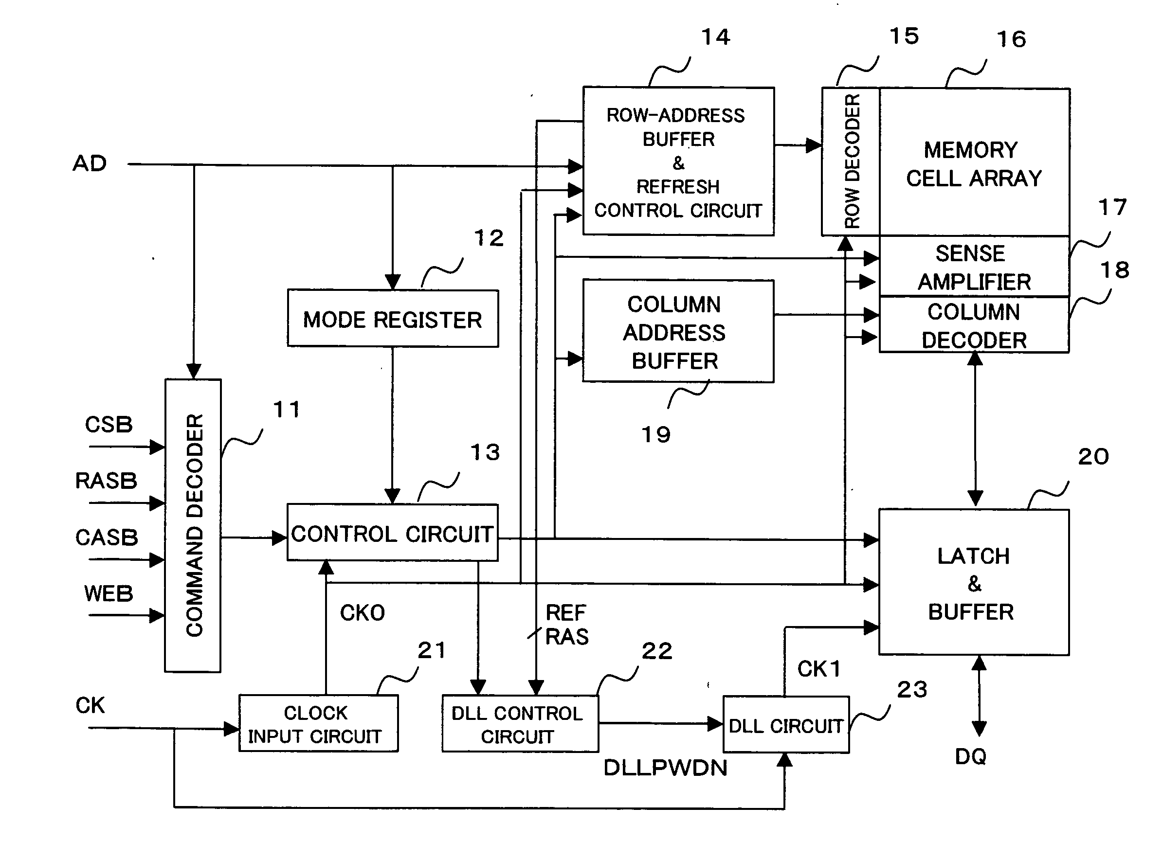
[0045]FIG. 1 is a block diagram illustrating the structure of a semiconductor storage device according to a first embodiment of the present invention. As shown in FIG. 1, the semiconductor storage device is an SDRAM and includes a command decoder 11, a mode register 12, a control circuit 13, a row-address buffer & refresh control circuit 14, a row decoder 15, a memory cell array 16, a sense amplifier 17, a column decoder 18, a column address buffer 19, a latch & buffer 20, a CK input circuit 21, a DLL control circuit 22 and a DLL circuit 23.
[0046] The command decoder 11 decodes a chip select signal CSB, a row-address strobe signal RASB, a column address strobe signal CASB, a write-enable signal WEB and an address signal AD and outputs a decoded signal, which is for setting various operating modes in the SDRAM, to the control circuit 13. On the basis of the decoded signal and the address signal AD, which has been loaded by a mode register 12, the control circuit 13 controls the row-...
second embodiment
[0057]FIG. 7 is a circuit diagram illustrating the DLL control circuit 22 according to a second embodiment of the present invention. Components identical with those shown in FIG. 5 are designated by like reference characters and need not be described again. The DLL control circuit 22 shown in FIG. 7 includes an inverter INV3 inserted between the data output terminal QT of the D-type flip-flop DFF1 in FIG. 5 and the other input terminal of the OR gate OR1.
[0058]FIG. 8 is a timing chart of the DLL control circuit 22 depicted in FIG. 7. In FIG. 8, the signal DLLPWDN controlled by the signals REF and RAS a low-level interval from the first falling edge of the signal RAS to the falling edge of the signal REF. In the first embodiment, the arrangement is such that the DLL circuit is caused to operate in the first half of the auto-refresh time period. In the second embodiment, however, it is so arranged that the DLL circuit is caused to operate in the latter half of the auto-refresh time p...
third embodiment
[0059]FIG. 9 is a circuit diagram illustrating the DLL control circuit 22 according to a third embodiment of the present invention. Components identical with those shown in FIG. 5 are designated by like reference characters and need not be described again. The DLL control circuit shown in FIG. 9 is devoid of the AND gate AND1 in FIG. 5 and has the signal RAS input directly to the clock input terminal input CLK of the D-type flip-flop DFF1. Further, the OR gate OR1 of FIG. 5 is eliminated and the circuit is provided with a NAND gate NAND1. The signal REF is input to one input terminal of the NAND gate NAND1, the data output terminal QT is connected to the other input terminal, and the output terminal of the NAND gate NAND1 outputs the signal DLLPWDN to the DLL circuit 23.
[0060]FIG. 10 is a timing chart of the DLL control circuit illustrated in FIG. 9. As shown in FIG. 10, the signal DLLPWDN controlled by the signals REF and RAS assumes the low level from the first rising edge of the...
PUM
 Abstract
Description
Claims
Application Information