Method and circuit configuration for refreshing data in a semiconductor memory

Inactive Publication Date: 2005-05-19
POLARIS INNOVATIONS
View PDF17 Cites 20 Cited by
  • Summary
  • Abstract
  • Description
  • Claims
  • Application Information

AI Technical Summary

Benefits of technology

[0012] One embodiment provides a method for reducing current in a semiconductor memory device comprising a plurality of rows of memory cells. The method generally includes maintai

Problems solved by technology

As a result, refreshing memory cells is a power-consuming routine.
However, one disadvantage with PAR schemes, is that the performance of multiple bank memories, such as DRAMs and double data rate (DDR) DRAMs, is often optimized by interleaving operations involving different banks, such that certain latencies associated with accessing each bank are hidden.
I

Method used


Image

  • Method and circuit configuration for refreshing data in a semiconductor memory
  • Method and circuit configuration for refreshing data in a semiconductor memory
  • Method and circuit configuration for refreshing data in a semiconductor memory

Examples


Example

[0025] To facilitate understanding, identical reference numerals have been used, where possible, to designate identical elements that are common to the figures.

[0026] It is to be noted, however, that the appended drawings illustrate only exemplary embodiments of this invention and are therefore not to be considered limiting of its scope, for the invention may admit to other equally effective embodiments.

DETAILED DESCRIPTION

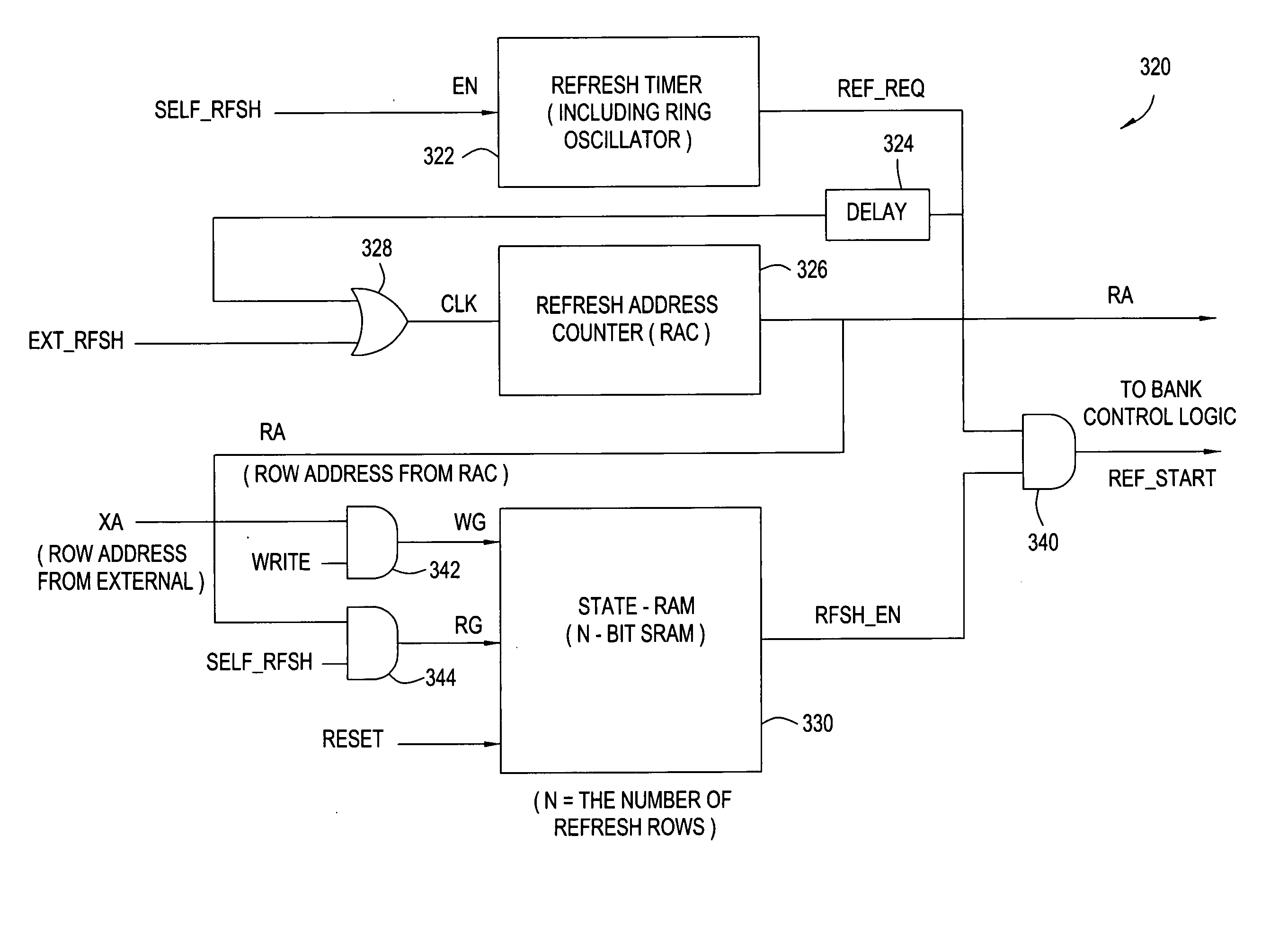
[0027] The present invention provides methods and circuit configurations for refreshing data in a semiconductor memory device in which only rows with memory cells that contain valid data are refreshed. For some embodiments, bits in a memory circuit (referred to herein as a state RAM) may be maintained to indicate which rows contain valid data. In other words, each bit in the state RAM may correspond to a refreshable row, with the state of the bit indicating whether a memory cell in the corresponding row has been written to since a reset event. When performing r...


PUM


Abstract

Methods and circuit configurations for refreshing data in a semiconductor memory device in which refresh operations are performed for a limited number of rows. The limited number of rows may include only those rows that contain valid data, for example, as determined by monitored write operations.

Description

BACKGROUND OF THE INVENTION [0001] 1. Field of the Invention [0002] The present invention generally relates to semiconductor memory devices and, more particularly, to dynamic semiconductor memory devices having memory cells that require refresh. [0003] 2. Description of the Related Art [0004] The evolution of sub-micron CMOS technology has resulted in an increasing demand for high-speed semiconductor memory devices, such as dynamic random access memory (DRAM) devices, pseudo static random access memory (PSRAM) devices, and the like. Herein, such memory devices are collectively referred to as DRAM devices. Such devices utilize memory cells consisting of one transistor and one capacitor. Due to leakage, the memory cells require periodic refreshing to protect data that is stored in the memory cell from corruption or decaying over time. The data stored in the memory cell is automatically restored to a full logic level when accessed (e.g., via a read or write operation), but must be peri...

Claims


Application Information

Patent Timeline
IPC IPC(8): G11C11/406
CPCG11C11/40622G11C11/406G11C11/40615G11C11/4072G11C2211/4065
Inventor OH, JONG-HOON
Owner POLARIS INNOVATIONS
Why Eureka
Try Eureka