Sample-and-Hold Circuit and Pipeline Ad Converter Using Same

Inactive Publication Date: 2009-08-13
SONY CORP
View PDF1 Cites 22 Cited by
  • Summary
  • Abstract
  • Description
  • Claims
  • Application Information

AI Technical Summary

Benefits of technology

[0042]The sample-and-hold circuit of the present invention switches the current source of an amplifier and the sizes of amplification use transistors in accordance with the operation mode by using switches and makes the operation current variable so can reduce an operation mean current.
[0043]Further, by using this sample-and-hold circuit in a pipeline AD converter, the power consumption can be reduced.
[0044]The sample-and-hold circuit of the present invention increases the output dynamic range and in addition can suppres

Problems solved by technology

On the other hand, along with the recent reduction of voltages, it has been becoming very difficult to vertically stack a plurality of transistors as shown in FIG. 3.
For this reason, there is a case where a folded configuration is employed, but this has

Method used


Image

  • Sample-and-Hold Circuit and Pipeline Ad Converter Using Same
  • Sample-and-Hold Circuit and Pipeline Ad Converter Using Same
  • Sample-and-Hold Circuit and Pipeline Ad Converter Using Same

Examples


embodiment 1

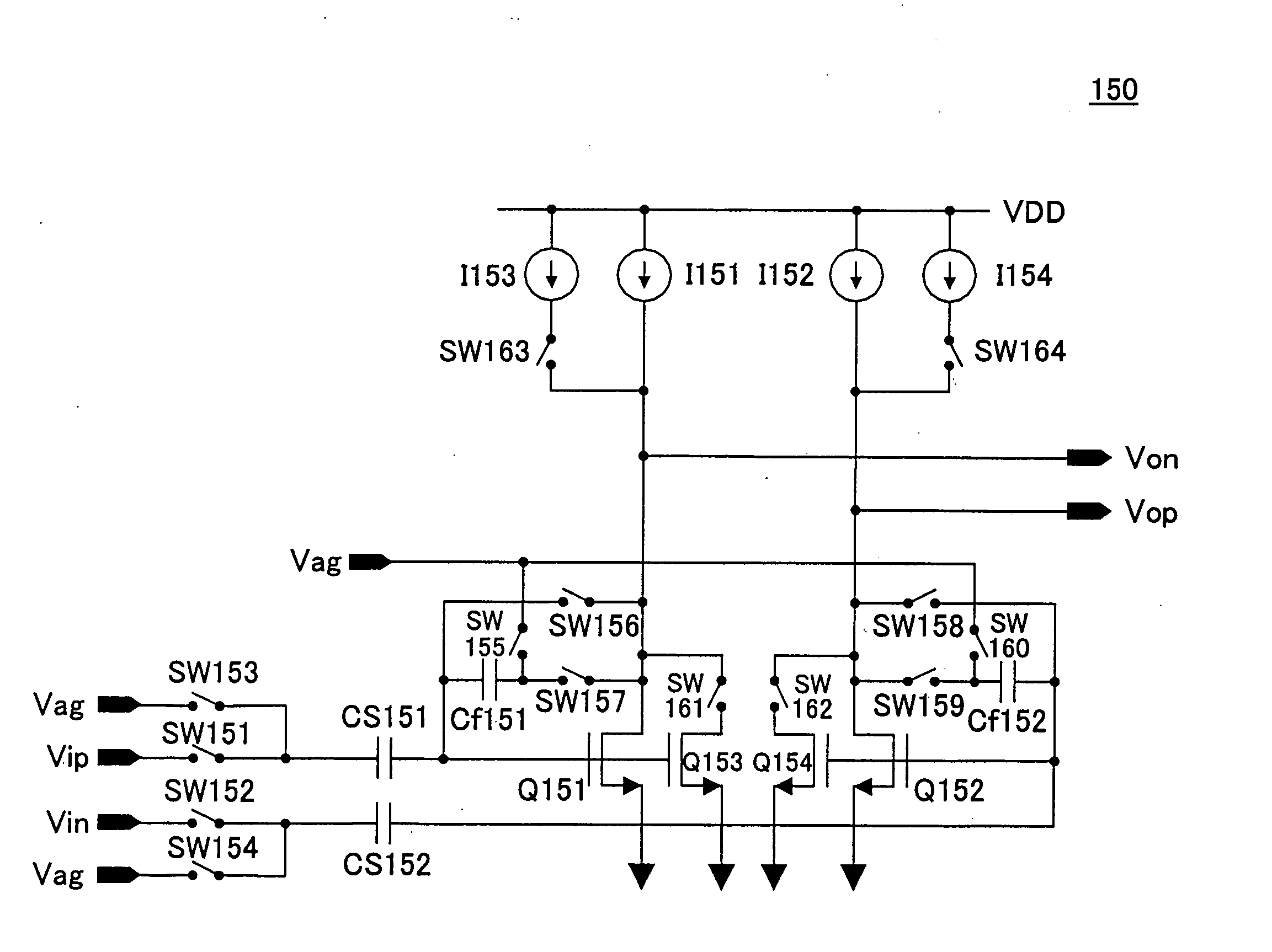
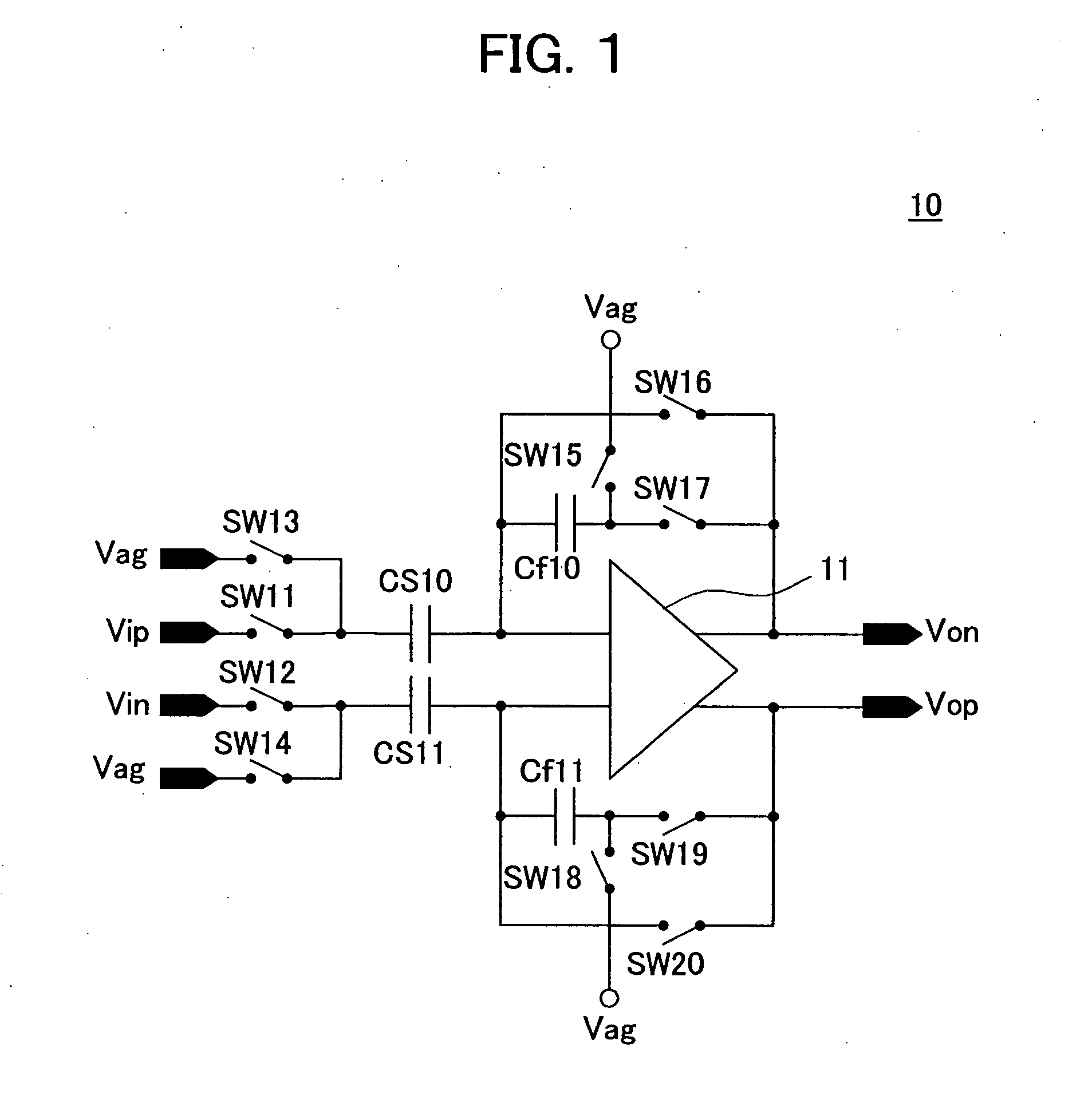
[0065]A sample-and-hold circuit 150 according to an embodiment of the present invention is shown in FIG. 5.

[0066]One side of a current source I151 is connected to the voltage source VDD, the other side is connected to the drain of an NMOS transistor Q151, and a current source I153 and a switch SW163 are serially connected in parallel to the current source I151. The current source I153 is the current source for flowing a current n times the current source I151. The source of the NMOS transistor Q151 is connected to the ground, an SW156 is connected between the gate and the drain. In parallel to this, a serially connected SW157 and capacitor Cf151 are connected. The common connection point of these capacitor Cf151 and SW157 is connected via SW155 to Vag.

[0067]A source grounded type NMOS transistor Q153 is provided in parallel to the NMOS transistor Q151 configuring a pseudo differential circuit, the gate of this is commonly connected to the gate of Q151, and the drain is connected via...

embodiment 2

[0095]Next, a sample-and-hold circuit 200 as another embodiment of the present invention is shown in FIG. 7. Here, elements indicating same configurations as those in FIG. 5 are served with same notations. Further, this sample-and-hold circuit 200 has a configuration obtained by adding a common mode feed forward (CMFF) circuit to the circuit formed by deleting a portion of FIG. 5.

[0096]Hereinafter, for simplifying the circuit configuration and its explanation, only one MOS transistor is shown as the source grounded transistor, but other MOS transistors may be connected in parallel by using switches, and switch (SW) and current source may be provided in parallel also in the constant current source corresponding to this.

[0097]The input of the CMFF circuit 202 is connected to Vip and Vin and connected also to Vag. The output of the CMFF circuit 202 is connected to the common connection point of the capacitor Cf151 and the SW157 and the common connection point of the capacitor Cf152 and...

embodiment 3

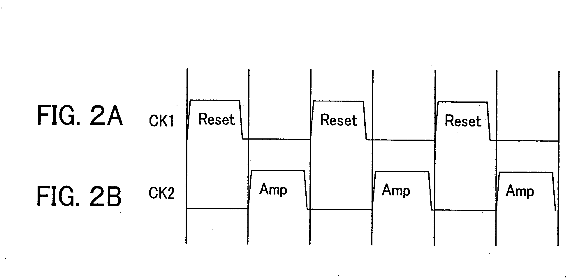
[0111]FIG. 8 shows a CMFF circuit 250 of the embodiment. The CMFF circuit 250 corresponds to the CMFF circuit 202 configured in the sample-and-hold circuit 200 explained before. The timing for explaining the operation thereof is shown in FIG. 9. Clock signals (CK3, CK4) supplied to the CMFF circuit 250 (202) operate as inverse phase clocks to the control clock signals (CK1, CK2) of the sample-and-hold circuit 200.

[0112]In FIG. 8, the input terminal supplied with Vin is connected to one end of an SW251, and the other end of the SW251 is connected to a capacitor CS250. Further, the common connection point of this SW251 and the capacitor CS250 is connected via an SW253 to the Vag.

[0113]The input terminal supplied with Vip is connected to one end of an SW252, and the other end of the SW252 is connected to a capacitor CS251. Further, the common connection point of this SW252 and the capacitor CS251 is connected via an SW254 to the Vag.

[0114]The other ends of the capacitors CS250 and CS25...


PUM


Abstract

A switched capacitor sample-and-hold circuit using a source grounded input operational amplifier, wherein a feed forward circuit or a feedback circuit is provided in the operational amplifier and connected to the feedback capacitor of the operational amplifier via switches, an input common voltage or a middle point voltage of outputs is detected, and a difference of the same from a reference voltage is previously charged in the feedback capacitor, thereby suppressing fluctuation of an output operation point at the time of amplification of the operational amplifier.

Description

TECHNICAL FIELD[0001]The present invention relates to a sample-and-hold circuit using switched capacitors and a pipeline AD converter using the same.BACKGROUND ART[0002]FIG. 1 shows a conventionally used basic S / H (sample-and-hold) circuit 10. The S / H circuit 10 is configured by an operational amplifier 11, switches SW11, SW12, SW13, SW14, SW15, SW16, SW17, SW18, SW19, and SW20, and switched capacitors comprised by capacitances CS10, CS11, Cf10, and Cf11.[0003]Vag is connected via the switch SW13 to one side of the capacitor CS10, and Vip is connected via the SW11 to one side of the capacitor CS10. The other terminal is connected to the first input of the operational amplifier 11.[0004]Further, Vin is connected via the SW12 to one side of the capacitor CS11, and Vag is connected via the SW14 to one side of the capacitor CS11. The other terminal is connected to the second input of the operational amplifier 11.[0005]The first output of the operational amplifier 11 is connected via the...

Claims


Application Information

Patent Timeline
IPC IPC(8): G11C27/02
CPCG11C27/026H03F3/45717H03M1/145H03F2203/45726H03M1/1245H03F2203/45634H03M1/14H03M1/12
Inventor ONO, KOICHISEGAMI, MASAHIRO
Owner SONY CORP
Why Eureka
Try Eureka