Manufacturing method of light emitting diode including current spreading layer

Inactive Publication Date: 2010-09-23
ELECTRONICS & TELECOMM RES INST
View PDF9 Cites 19 Cited by
  • Summary
  • Abstract
  • Description
  • Claims
  • Application Information

AI Technical Summary

Benefits of technology

[0011]As described above, the 2-DEG and 2-DHG structures formed by the hetero-junction are used for the n- and p-type current spreading layers, so that the current quickly flows on two-dimensional plane as compared with the bulk structure of the existing n-GaN and p-GaN. Thus, the partial current crowding and the non-uniform light emission, which arise in the existing large-sized light emitting diodes, are reduced, and thus it is possible to manufacture a large-sized light emitting diodes.
[0012]Further, in the foregoing configurations, the metal electrode is inserted within the trench, so that the metal electrode can be planarized by the following process as

Problems solved by technology

However, the emission properties of III-nitrides are difficult in increasing quantum efficiency due to a large lattice mismatch and growth temperature difference between the active layer and the electrode layer.
Furthermore, in t

Method used


Image

  • Manufacturing method of light emitting diode including current spreading layer
  • Manufacturing method of light emitting diode including current spreading layer
  • Manufacturing method of light emitting diode including current spreading layer

Examples


Embodiment Construction

[0036]Hereinafter, exemplary embodiments of the present invention will be described in detail. However, the present invention is not limited to the embodiments disclosed below, but can be implemented in various forms. Therefore, the following embodiments are described in order for this disclosure to be complete and enabling to those of ordinary skill in the art.

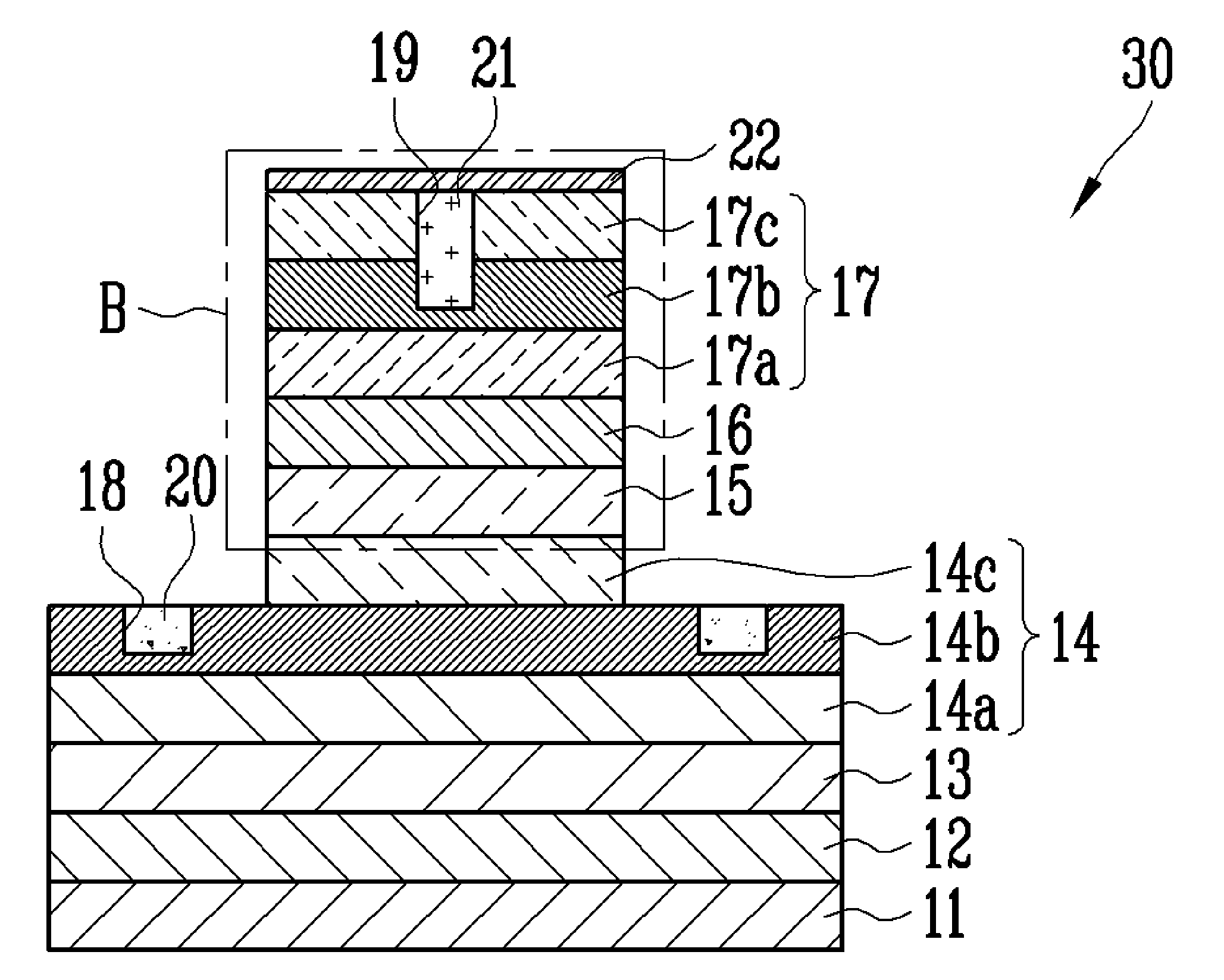
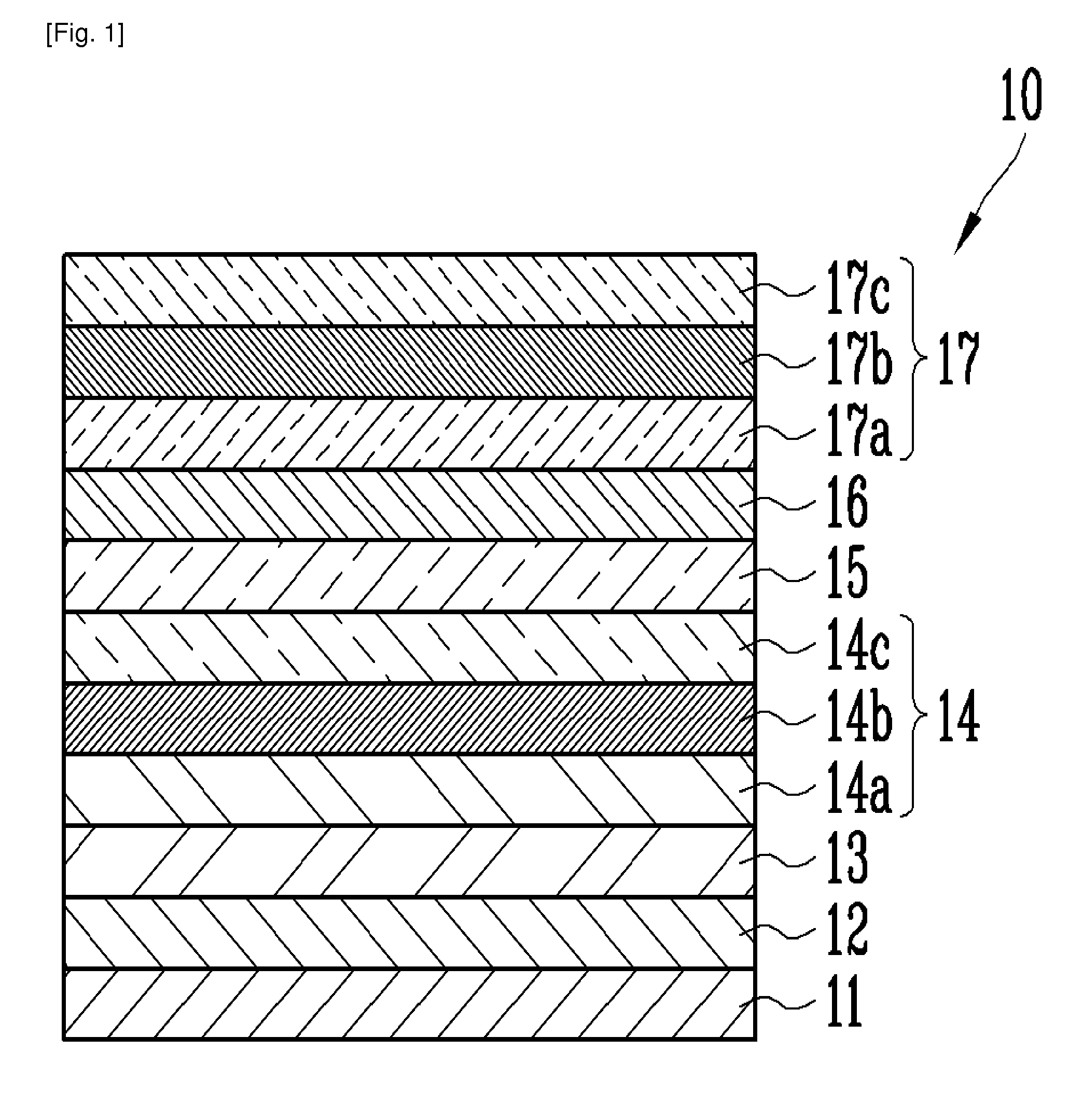
[0037]FIG. 1 is a cross-sectional view illustrating an epitaxial structure of the nitride light emitting diode according to an exemplary embodiment of the present invention. Referring to FIG. 1, the nitride light emitting diode 10 includes a substrate 11, a buffer layer 12 formed on the substrate 11, a GaN support layer 13 formed on the buffer layer 12, an n-type electrode layer 14 formed on the GaN support layer 13, an active layer 15 formed on the n-type electrode layer 14, a p-type cladding layer 16 formed on the active layer 15, and a p-type electrode layer 17 formed on the p-type cladding layer 16.

[0038]For example, the ...


PUM


Abstract

Provided is a method of manufacturing a light emitting diode using a nitride semiconductor, which including the steps of: forming n- and p-type current spreading layers using a hetero-junction structure; forming trenches by dry-etching the n- and p-type current spreading layers; forming an n-type metal electrode layer in the trench of the n-type current spreading layer; forming a p-type metal electrode layer in the trench of the p-type current spreading layer; and forming a transparent electrode layer on the p-type metal electrode layer, thereby improving current spreading characteristics as compared with the conventional method of manufacturing the light emitting diode, and enhancing operating characteristics of the light emitting diode.

Description

TECHNICAL FIELD[0001]The present invention relates to a method of manufacturing a light emitting diode using III-group nitride semiconductors including nitrogen and III-group elements such as gallium (Ga), aluminum (Al), Indium (In), and in particularly, to a method of manufacturing a nitride light emitting diode including process of forming a 2-dimensional electron gas (2-DEG) layer and a 2-dimensional hole gas (2-DHG) layer which have low resistivity and high surface electron / hole concentration in a process of forming n- and p-type electrodes.BACKGROUND ART[0002]In general, III-nitride compound semiconductors have a direct bandgap, which is capable of controlling wavelengths from visible to ultraviolet, and excellent physical properties of high thermal and chemical stability, high electron mobility, and high saturation electron velocity, as compared with the GaAs and InP-related compound semiconductors. With these properties, the III-nitrides have been widely applied to the optica...

Claims


Application Information

Patent Timeline
IPC IPC(8): H01L33/00H01L33/14H01L33/20H01L33/32H01L33/38
CPCH01L33/14H01L33/20H01L2933/0016H01L33/38H01L33/32
Inventor BAE, SUNG BUM
Owner ELECTRONICS & TELECOMM RES INST
Why Eureka
Try Eureka