Fingerprint Sensing device using pulse processing

Active Publication Date: 2007-04-26
QI BAOHUA
View PDF2 Cites 14 Cited by
  • Summary
  • Abstract
  • Description
  • Claims
  • Application Information

AI Technical Summary

Benefits of technology

[0009] Since no voltage level signals are employed for comparison and reference, the circuits in the present invention can be configured insensitive to the change or fluctuat

Problems solved by technology

When a serial or parallel communication is used, the sensing time for the binary image sensors is determined by discharging time of sensing

Method used


Image

  • Fingerprint Sensing device using pulse processing
  • Fingerprint Sensing device using pulse processing
  • Fingerprint Sensing device using pulse processing

Examples


Embodiment Construction

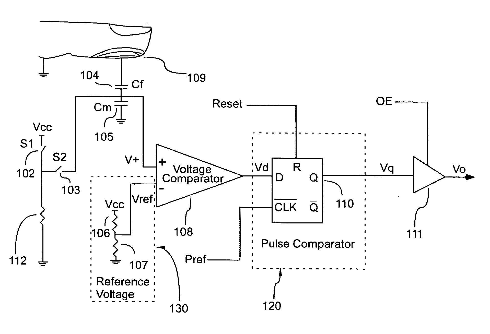
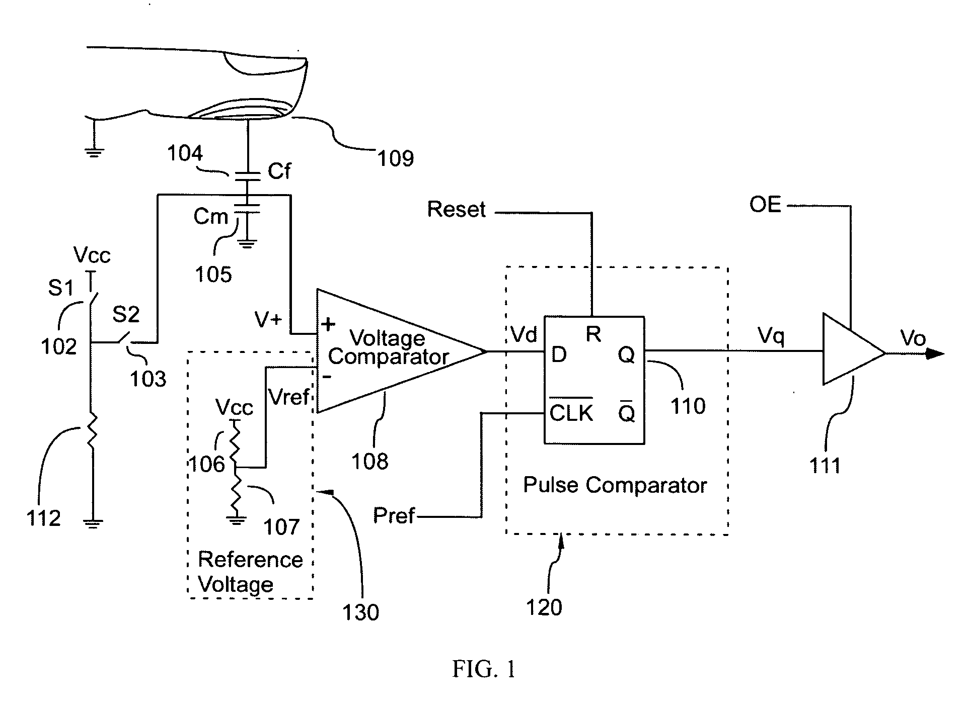
[0017] The numerous innovative teachings of the present application will be described with particular reference to the presently preferred embodiment. However, it should be understood that this class of embodiments provides only a few examples of the many advantageous uses of the innovative teachings herein. In general, statements made in the specification of the present application do not necessarily delimit any of the various claimed inventions. Moreover, some statements may apply to some inventive features but not to others. Detailed descriptions of known functions and constructions unnecessarily obscuring the subject matter of the present invention have been omitted for clarity. An equivalent circuit diagram of the present fingerprint sensors that generates binary images is shown in FIG. 1. A resistor 112 is connected to a voltage source Vcc through a switch S1 (102). A switch S2 (103) is used to connect the resistor 112 to the positive input of a voltage comparator 108, and the...


PUM


Abstract

A fingerprint sensing device that measures the capacitance between an array of electrode plates and finger skin using pulse processing, in which pulse width rather than voltage level, is used for capacitance measurement and digital signal conversion. A pulse, the width of which is compared and adjusted with that of a reference pulse, is generated when voltage at sensing electrodes in discharging is compared with a reference voltage. The comparison results are then digitalized in a grade image sensor or output directly in a binary image sensor. The sensor can communicate with a CPU using serial communication, parallel communication, or memory map scheme. Since no A/D is used, there is no extra time and hardware cost for the conversion from analog signals to digital signals. Due to the pulse processing nature, the circuits can be configured insensitive to the change or fluctuation in voltage supply. This feature enables the sensing device work with a variety of voltages, and thus it can be better used in portable, battery powered or passive devices.

Description

FIELD OF THE INVENTION [0001] This present application claims priority from U.S. provisional application No. 60 / 729,670 having the same tile as the present invention and filed on Oct. 24, 2005. This invention relates to an apparatus for fingerprint sensing, more particularly, to a capacitive fingerprint sensor using pulse-processing method. BACKGROUND OF THE INVENTION [0002] As a biometric technique, fingerprint based identification has been successfully used in numerous applications, such as access control for buildings, verification of personal identity for portable communication, computing and network interface devices, and forensics. An electronic fingerprint device generally includes a fingerprint-sensing device that acquires fingerprint from a finger surface, and a fingerprint recognition device, which is used to process the data obtained with the fingerprint-sensing device. A variety of methods, including optical, capacitive, thermal, RF-imaging, and mechanical sensing, have ...

Claims


Application Information

Patent Timeline
IPC IPC(8): G06K9/00
CPCG06K9/0002G06V40/1306
Inventor QI, BAOHUA
Owner QI BAOHUA
Why Eureka
Try Eureka