MOS varactor property detection method and MOS varactor manufacturing method using the same

a technology of mos varactor and manufacturing method, which is applied in the testing/measurement of semiconductor/solid-state devices, computation using non-denominational number representation, instruments, etc., can solve the problems of low accuracy when the same parameters are applied to elements having different areas, and it is difficult to simultaneously satisfy various capacitor sizes in one model

Inactive Publication Date: 2007-04-26
DONGBU ELECTRONICS CO LTD
View PDF5 Cites 16 Cited by
  • Summary
  • Abstract
  • Description
  • Claims
  • Application Information

AI Technical Summary

Benefits of technology

[0019] According to the method, a MOS varactor model equation applicable to various areas and perimeters of a capacitor is proposed, so that it i

Problems solved by technology

Such a MOS varactor model equation shows high accuracy for a single area, but shows low accuracy when the same parameters are applied to elements having different ar

Method used


Image

  • MOS varactor property detection method and MOS varactor manufacturing method using the same
  • MOS varactor property detection method and MOS varactor manufacturing method using the same
  • MOS varactor property detection method and MOS varactor manufacturing method using the same

Examples


Embodiment Construction

[0024] Hereinafter, the preferred embodiment of the present invention will be described in detail with reference to the accompanying drawings.

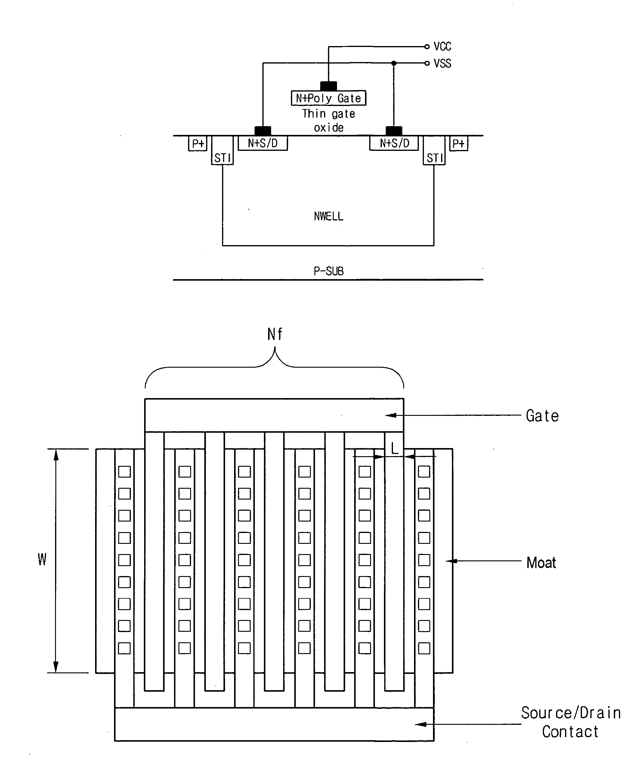
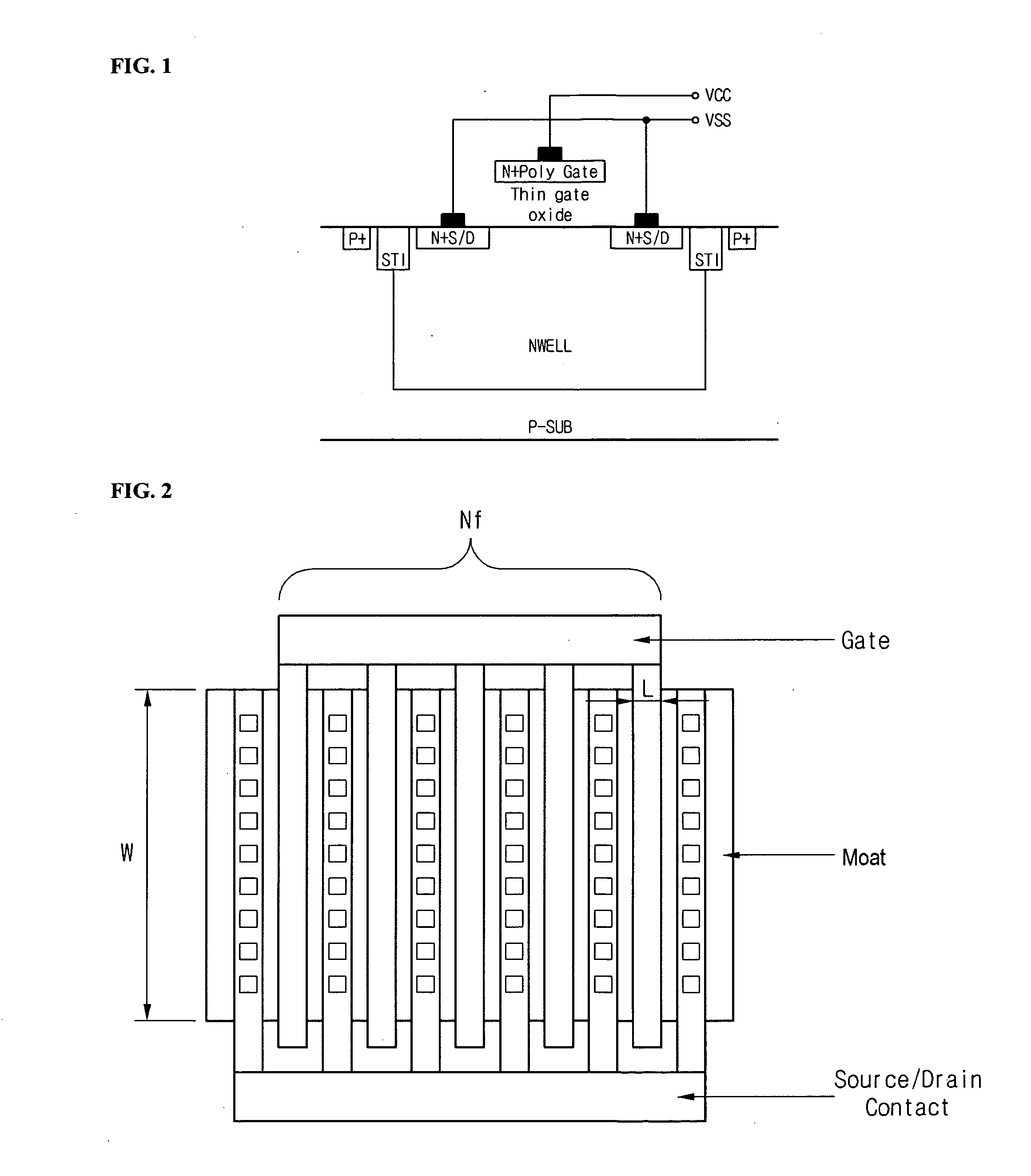
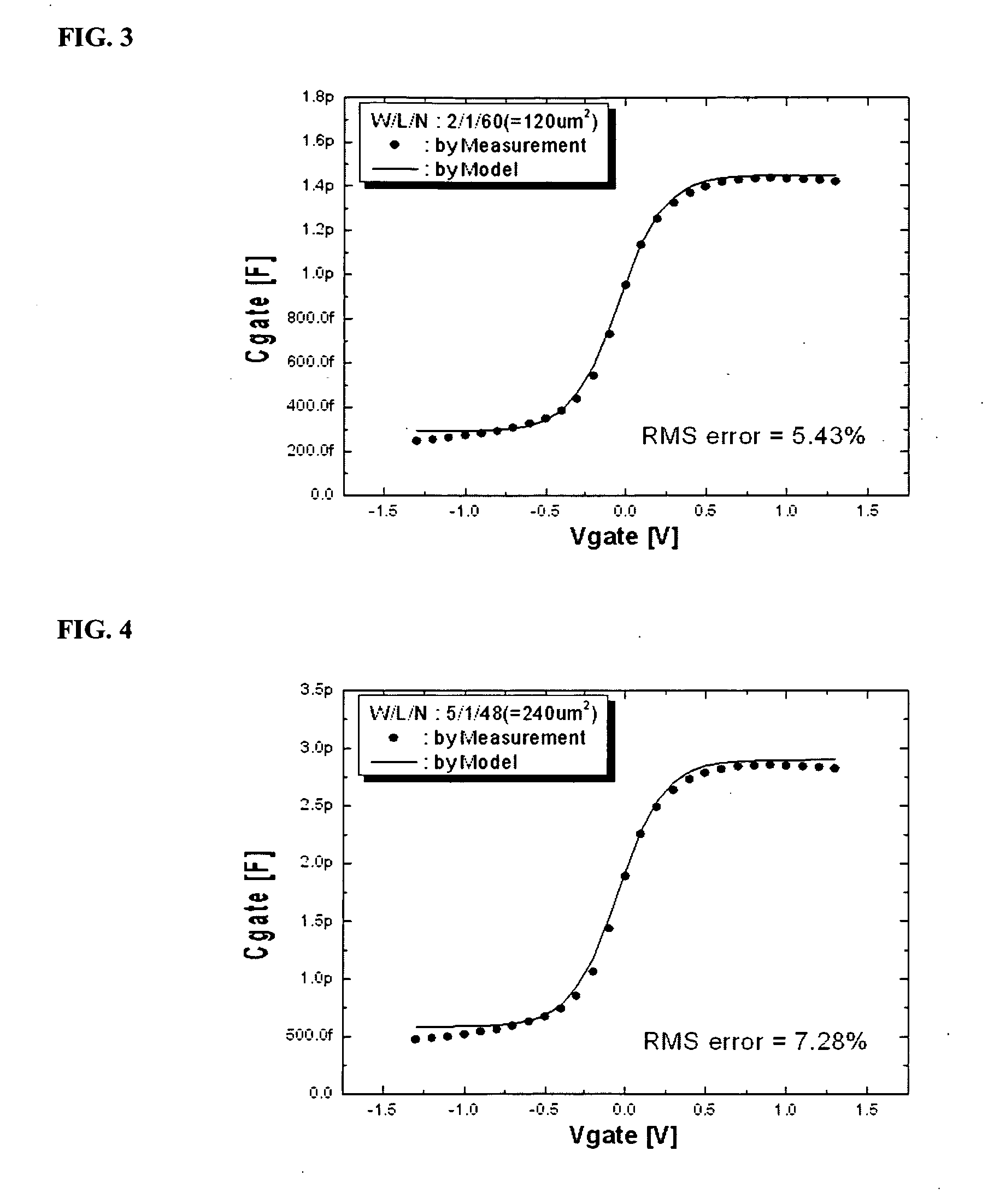
[0025] The present invention incorporates the fact that, in establishing a MOS varactor model equation, capacitance has both an area component and a perimeter component for each structure as expressed by equation 2.

Cgate=Cigate×Area+Cpgate×Perimeter  Equation 2:

[0026] In equation 2, Cigate denotes intrinsic gate capacitance and Cpgate denotes perimeter gate capacitance. That is, Cigate is the capacitance of an area component of a gate, and Cpgate is the capacitance of a perimeter component of the gate. The C-V characteristics of Cigate and Cpgate may be expressed by equations 3 and 4. Equation⁢ ⁢3⁢:Cigate=Cigmin⁢ ⁢0+dCigo×[1+tanh⁡(Vg-dVigs⁢ ⁢0Vignorm)]Equation⁢ ⁢4⁢:Cpgate=Cpgmin⁢ ⁢0+dCpgo×[1+tanh⁡(Vg-dVpgs⁢ ⁢0Vpgnorm)]

[0027] In equations 3 and 4, Cig min 0, dCigo, dVigs0 and Vignorm denote intrinsic gate capacitance coefficients, and CPg m...


PUM


Abstract

Disclosed is a method for detecting properties of a Metal Oxide Silicon (MOS) varactor, which includes: establishing a MOS varactor model equation in conjunction with an area of a gate; calculating values of the coefficients of the MOS varactor model equation through measurements for test materials; and extracting the properties of a capacitor of the MOS varactor using the calculated values of the coefficients. According to the method, the MOS varactor model equation can be expressed by Cgate=[Cigate×Area+Cpgate×Perimeter]×N, wherein, Cgate denotes gate capacitance for voltage applied to the gate, Cigate denotes intrinsic gate capacitance, Cpgate denotes perimeter gate capacitance, and N denotes the number of gate fingers. The MOS varactor model equation can be applicable to various sized capacitors, so that it is possible to estimate a gate capacitance for voltage applied to a gate, considering the differences due to the surface shapes of a device.

Description

RELATED APPLICATION(S) [0001] This application claims the benefit, under 35 U.S.C. §119(e), of Korean Patent Application Number 10-2005-0100143 filed Oct. 24, 2005, which is incorporated herein by reference in its entirety. FIELD OF THE INVENTION [0002] The present invention relates to a method for detecting properties of a Metal Oxide Silicon (MOS) varactor and a method for manufacturing the MOS varactor by using the same, and more particularly, to a method for detecting properties of a MOS varactor, which can precisely detect the properties of a MOS varactor regardless of the area and perimeter of a gate and the number of gate fingers, and a method for manufacturing the MOS varactor by using the same. BACKGROUND OF THE INVENTION [0003] With the recent development of wireless mobile communication, the importance of RF application devices has increased. Accordingly, an accumulation mode MOS varactor has been used in applications requiring a wide tuning range such as with a Voltage C...

Claims


Application Information

Patent Timeline
IPC IPC(8): H01L21/338
CPCH01L29/93H01L29/94H01L22/00
Inventor CHOI, JUNG HYUN
Owner DONGBU ELECTRONICS CO LTD
Why Eureka
Try Eureka