Method of making an inverted-T channel transistor

a transistor and inverter technology, applied in the field of integrated circuits, can solve the problems of inability to adjust the current drive of the transistor, general inapplicability, and fin heigh

Active Publication Date: 2007-04-26
NXP USA INC
View PDF20 Cites 154 Cited by
  • Summary
  • Abstract
  • Description
  • Claims
  • Application Information

AI Technical Summary

Problems solved by technology

One of the difficulties, however, has been the ability to adjust the current drive of the transistors, especially to increase the current drive.
One way to increase the channel width is to increase the fin height, but that is generally not practical because the fin height is generally selected to the maximum practical height and the difficulties with the methods that are able to alter fin heights.
The space between fins is desirably small but how small is limited by the pitch limitations of the lithography.

Method used


Image

  • Method of making an inverted-T channel transistor
  • Method of making an inverted-T channel transistor
  • Method of making an inverted-T channel transistor

Examples


Embodiment Construction

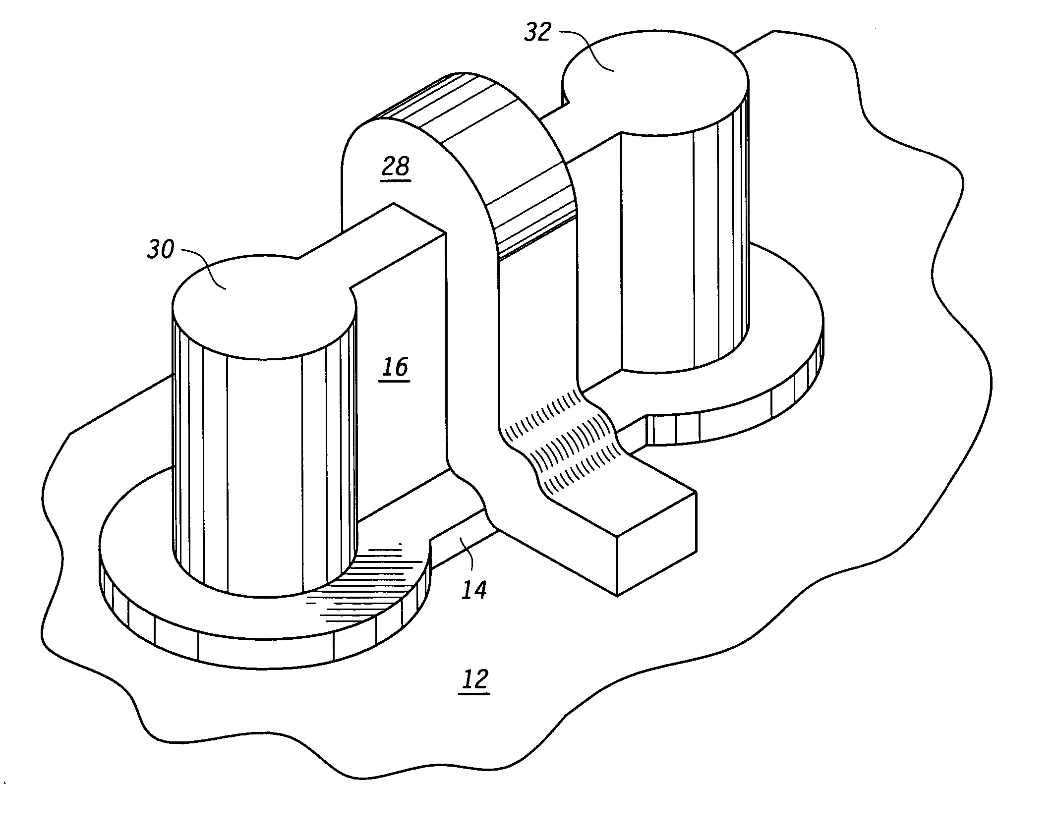
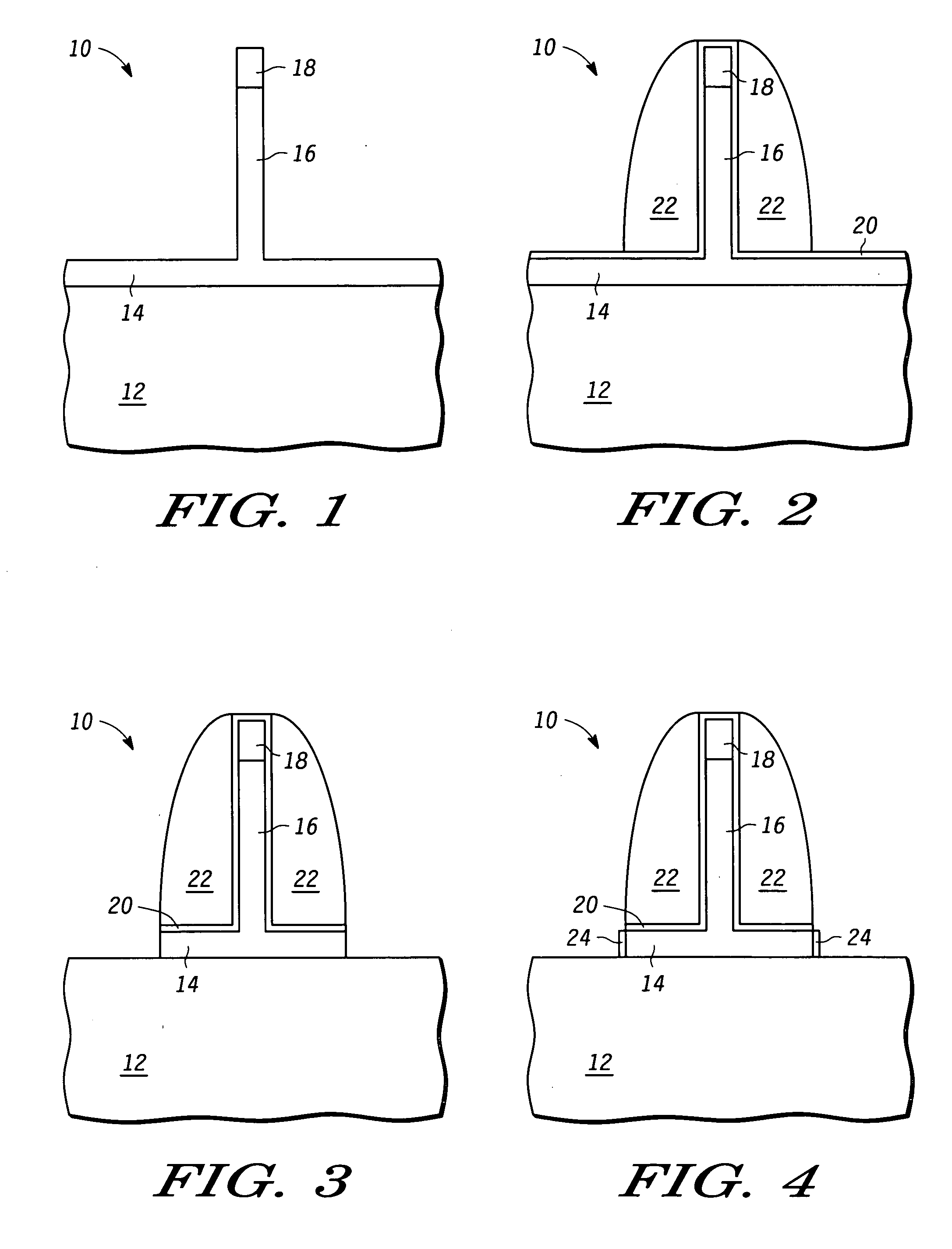
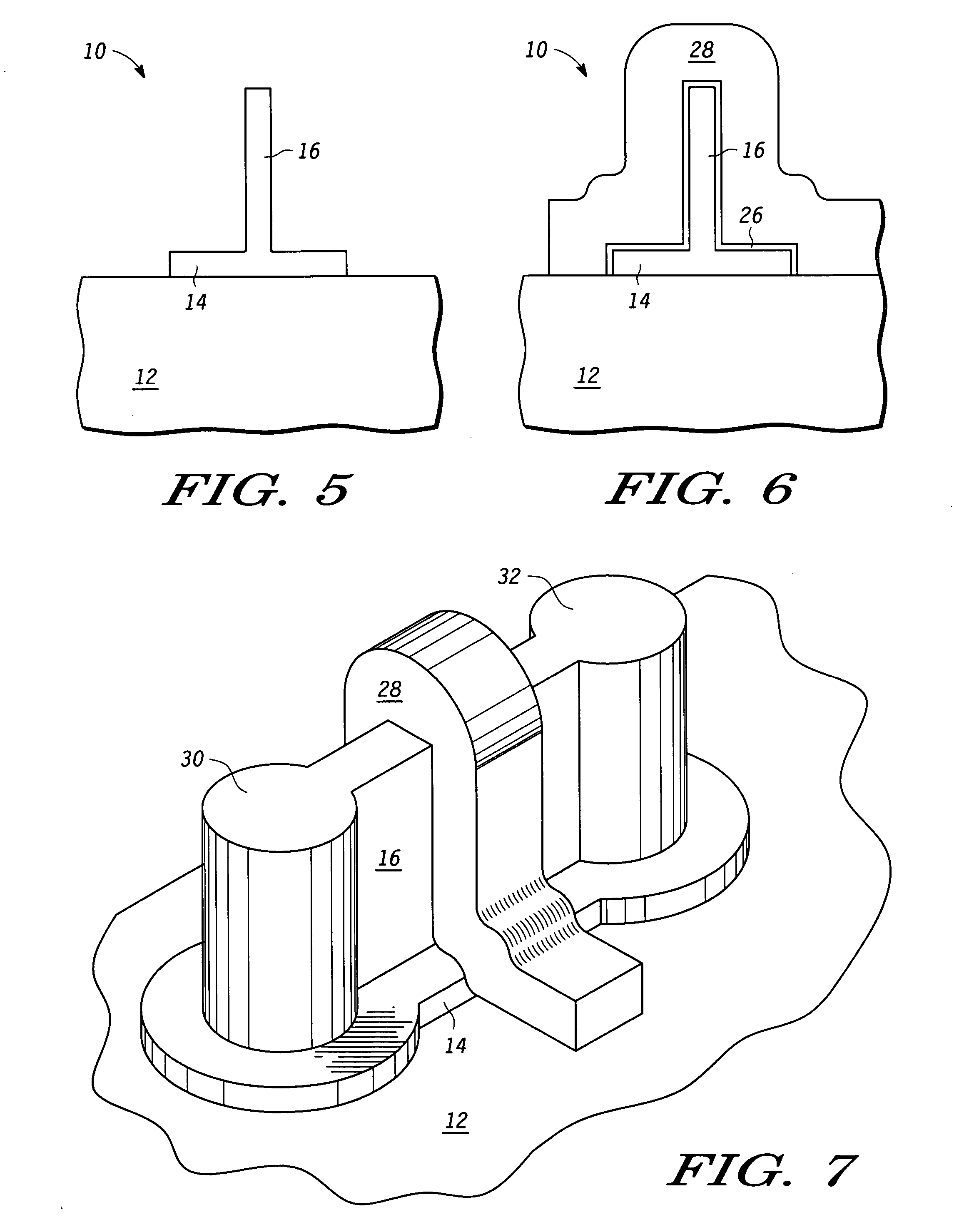
[0023] In one aspect a FinFET is made with a lateral extension of the channel so as to increase the current drive of the FinFET. A lateral extension extends adjacent to the fin of FinFET along the surface of the substrate. The gate that overlies the fin also overlies the lateral extension. The lateral extension is defined by a sidewall spacer. The fin is formed by an etch that leaves, in addition to the fin, a floor of semiconductor material that is left over the substrate. The sidewall spacer is formed on both sides of the fin to act as a mask in an etch of the floor of the semiconductor material to leave the lateral extension. The lateral extension is selectable within the range of sidewall spacers widths. Using conventional sidewall formation techniques, the width is easily adjustable from 50 to 1000 Angstroms. The lateral extension thus results in increased current drive that is selectable but not limited to increments corresponding to the fin height. This is better understood b...


PUM


Abstract

A method for creating an inverse T field effect transistor is provided. The method includes creating a horizontal active region and a vertical active region on a substrate. The method further comprises forming a sidewall spacer on a first side of the vertical active region and a second side of the vertical active region. The method further includes removing a portion of the horizontal active region, which is not covered by the sidewall spacer. The method further includes removing the sidewall spacer. The method further includes forming a gate dielectric over at least a first part of the horizontal active region and at least a first part of the vertical active region. The method further includes forming a gate electrode over the gate dielectric. The method further includes forming a source region and a drain region over at least a second part of the horizontal active region and at least a second part of the vertical active region.

Description

RELATED APPLICATIONS [0001] This application is related to the following: [0002] U.S. patent application Ser. No. 11 / 047,543, titled “Hybrid-Fet and Its Application As SRAM,” by Mathew, assigned to the assignee hereof, and filed Jan. 31, 2005; and [0003] U.S. patent application docket number SC14314TP, titled “Multiple Device Types Including an Inverted-T Channel Transistor and Method Therefor,” by Mm et al., assigned to the assignee hereof, and filed even date herewith.FIELD OF THE INVENTION [0004] This invention relates to integrated circuits, and more particularly, to a method of making inverted-T channel transistors. BACKGROUND OF THE INVENTION [0005] The use of FinFETs is very attractive for manufacturing for increasing the density and electrical characteristics of MOS transistors. The fin rises above a substrate to function as the channel so that a major portion of the transistor is vertical and not lateral. The channel direction is lateral but in a structure that is above the...

Claims


Application Information

Patent Timeline
Patent Type & Authority Applications(United States)
IPC IPC(8): H01L21/338
CPCH01L21/823431H01L27/11H01L27/1104H01L29/66795H01L29/785H10B10/00H10B10/12H01L29/76H01L21/18
Inventor MATHEW, LEOMORA, RODE R.
Owner NXP USA INC
Why Eureka
Try Eureka