
Method and system for mapping netlist of integrated circuit to design

a technology of integrated circuits and netlists, applied in the field of integrated circuits, can solve the problem of still fully decoupling of the slice, and achieve the effect of reducing the sum of wire length

Inactive Publication Date: 2007-04-26
BELL SEMICON LLC
View PDF6 Cites 4 Cited by
  • Summary
  • Abstract
  • Description
  • Claims
  • Application Information

AI Technical Summary

Benefits of technology

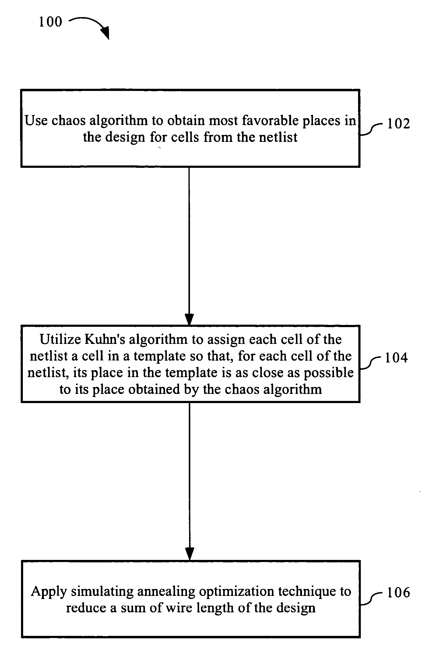
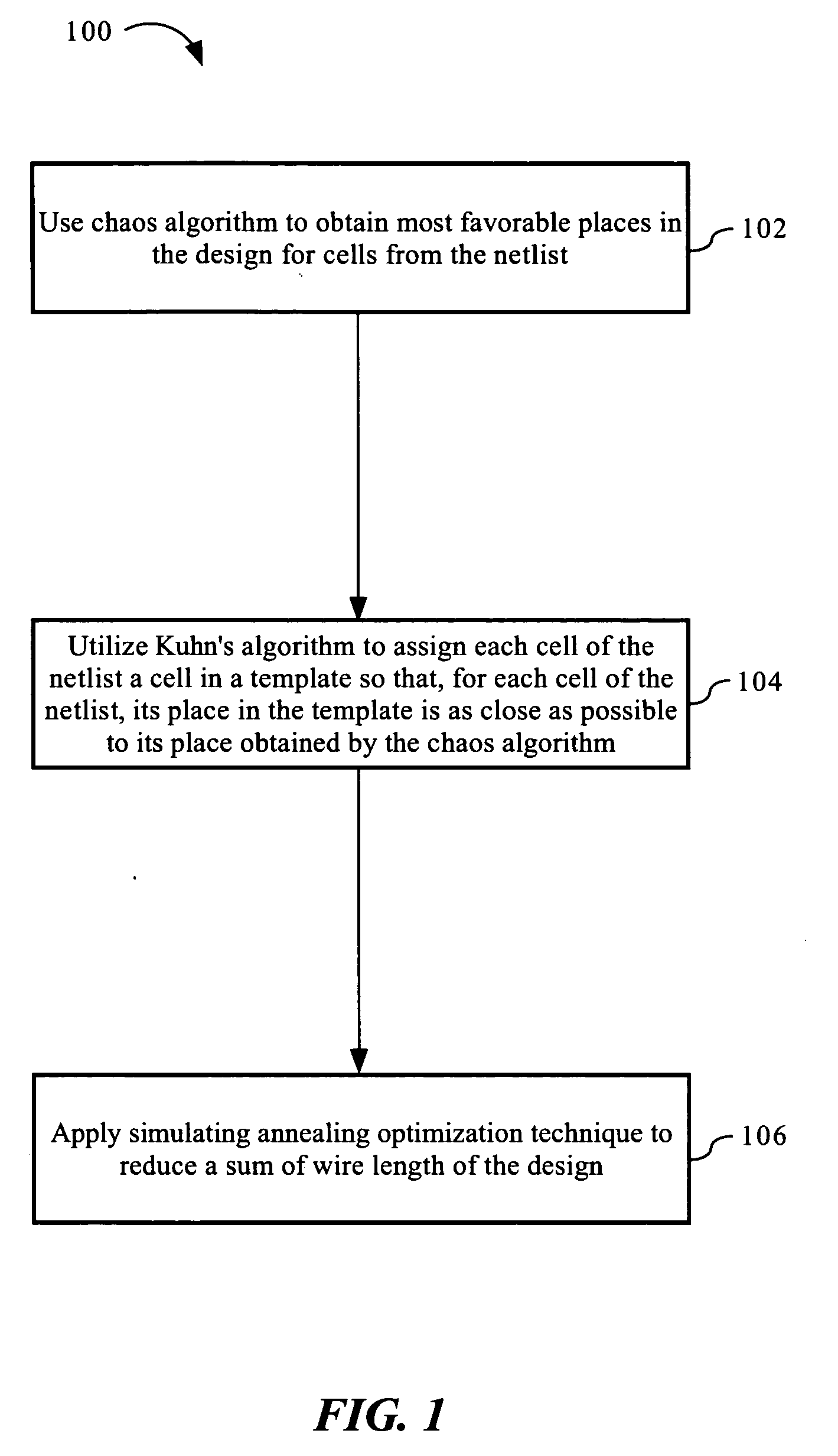
"The present invention provides a method for mapping a netlist of an integrated circuit to a design using a combination of techniques such as Chaos algorithm, Kuhn's algorithm, and simulating annealing optimization technique. This method helps to reduce the wire length of the design and improve its overall performance. The invention also provides a system and computer-readable medium for implementing this mapping process."

Problems solved by technology

However, a slice is still fully decoupled because the customer has not yet introduced the function into the slice.
The problem of mapping a netlist to a design, which includes cells with predefined locations, often rises up during the development of chips based on the RapidChip™ technology, and / or FPGA.

Method used


Image

  • Method and system for mapping netlist of integrated circuit to design
  • Method and system for mapping netlist of integrated circuit to design
  • Method and system for mapping netlist of integrated circuit to design

Examples


Embodiment Construction

[0016] Reference will now be made in detail to the presently preferred embodiments of the invention, examples of which are illustrated in the accompanying drawings.

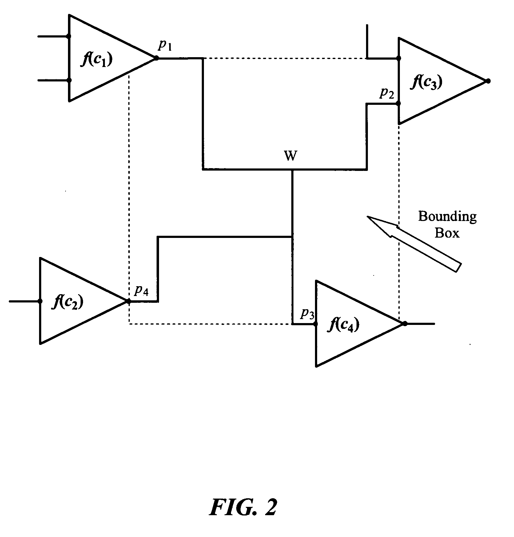
[0017] Consider a set (called a template design or template) T of cells and pins with predefined locations in RRAM. T has no wires. Let N be a netlist such that it has cell types that are instantiated in T only. All the input and output pins of the netlist N are assigned to predefined pins of T. In order to obtain a design that implements the netlist N, pins of cells of T need be connected to pins of T that correspond to the pins of N by wires. The most natural solution to this problem is to assign each cell in the netlist N a cell in T and then connect by wires the corresponding pins of the assigned cells. Since the total wire length is an important consideration in IC design, the present invention presents a solution with the sum of wire length that is as minimal as possible. In the present invention, routing is not ma...


PUM


Abstract

The present invention provides a method for mapping a netlist of an integrated circuit to a design. The method includes steps as follows. Chaos algorithm is used to obtain most favorable places in the design for cells from the netlist. Kuhn's algorithm is utilized to assign each cell of the netlist a cell in a template so that, for each cell of the netlist, its place in the template is as close as possible to its place obtained by the chaos algorithm. Simulating annealing optimization technique is applied to reduce a sum of wire length of the design.

Description

FIELD OF THE INVENTION [0001] The present invention generally relates to the field of integrated circuits, particularly to a method and system for mapping a netlist of an integrated circuit to a design. BACKGROUND OF THE INVENTION [0002] Platform-based IC (integrated circuit) design is a powerful concept for coping with the increased pressure on time-to-market, design and manufacturing costs encountered in the current IC market. A platform is a large-scale, high-complexity semiconductor device that includes one or more of the following elements: (1) memory; (2) a customizable array of transistors; (3) an IP (intellectual property) block; (4) a processor, e.g., an ESP (embedded standard product); (5) an embedded programmable logic block; and (6) interconnect. RapidChip™ developed by LSI Logic Corp. is an instance of a platform. The basic idea behind the platform-based design is to avoid designing and manufacturing a chip from scratch. Some portion of the chip's architecture is predef...

Claims


Application Information

Patent Timeline
Patent Type & Authority Applications(United States)
IPC IPC(8): G06F17/50
CPCG06F17/5077G06F2217/64G06F30/394G06F2115/06
Inventor ANDREEV, ALEXANDER E.PANTELEEV, PAVELNIKITIN, ANDREY A.
Owner BELL SEMICON LLC
Learn More