Liquid crystal display device

a liquid crystal display and display device technology, applied in non-linear optics, instruments, optics, etc., can solve the problems of short circuit between the opposing electrode and the pixel electrode, and the thickness of the coated film becomes considerably thin in the through hole portion having a large height difference,

Active Publication Date: 2007-05-03
PANASONIC LIQUID CRYSTAL DISPLAY CO LTD +1
View PDF5 Cites 33 Cited by
  • Summary
  • Abstract
  • Description
  • Claims
  • Application Information

AI Technical Summary

Benefits of technology

[0026] The liquid crystal display device of the invention enables to prevent short circuits

Problems solved by technology

The panel is also required to be flat considering a possible problem of domain generation due to not enough rubbing treatment in the post processing.
With this method, however, the thickness of the coated film beco

Method used


Image

  • Liquid crystal display device
  • Liquid crystal display device
  • Liquid crystal display device

Examples


Embodiment Construction

[0041] In the below, an embodiment of the invention is described in detail by referring to the accompanying drawings.

[0042] Note that, in all of the diagrams for use for illustrating the embodiment, any component having the same function and capability is under the same reference numeral, and not described twice.

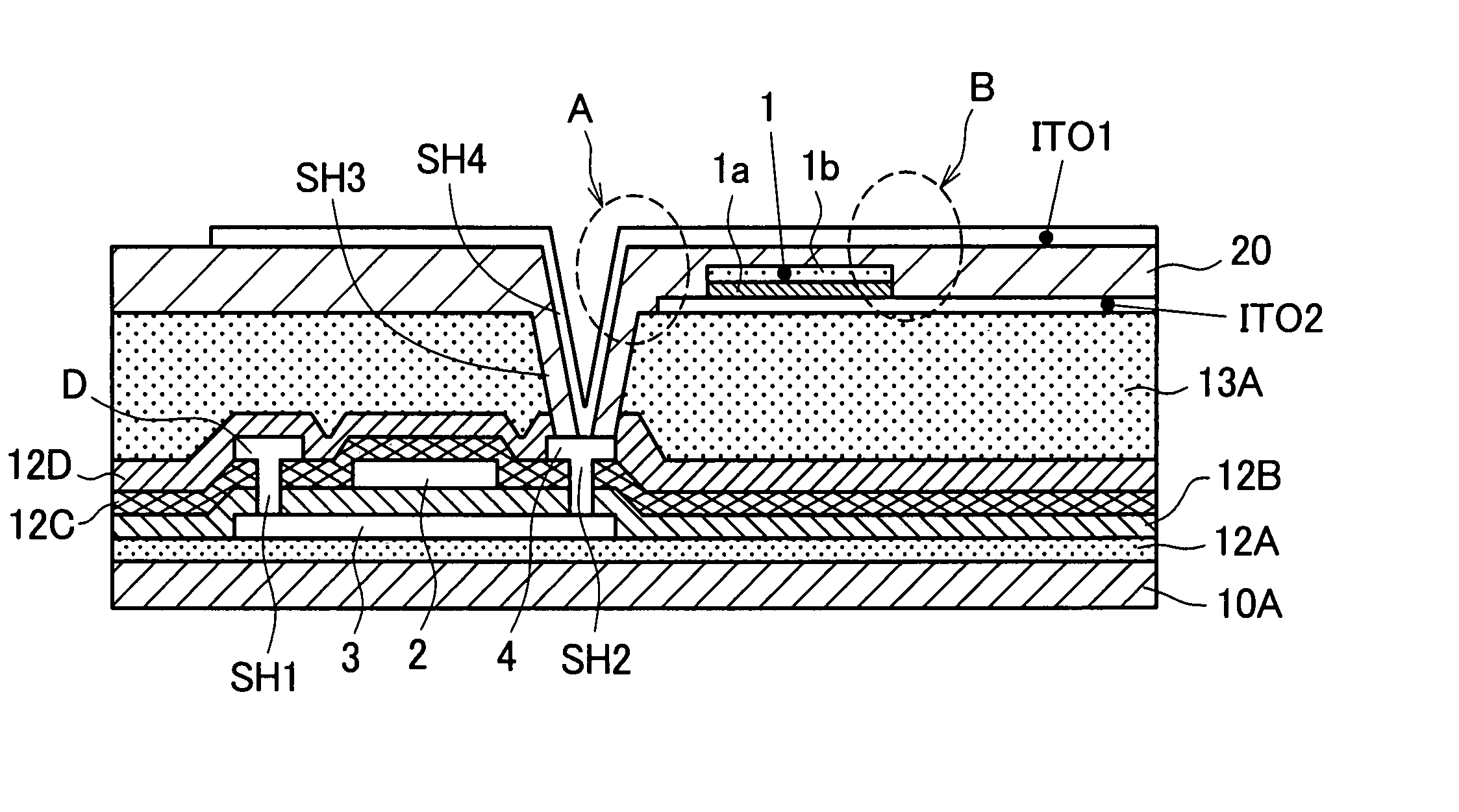
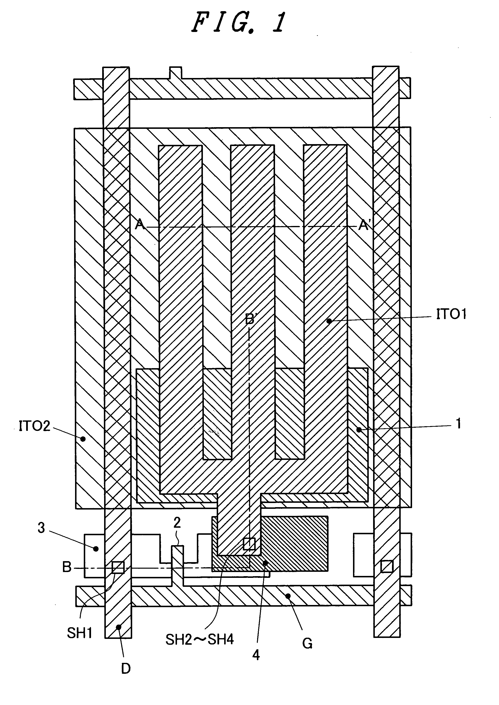
[0043]FIG. 1 is a plan view showing the configuration of a subpixel of a liquid crystal display panel in the embodiment of the invention.

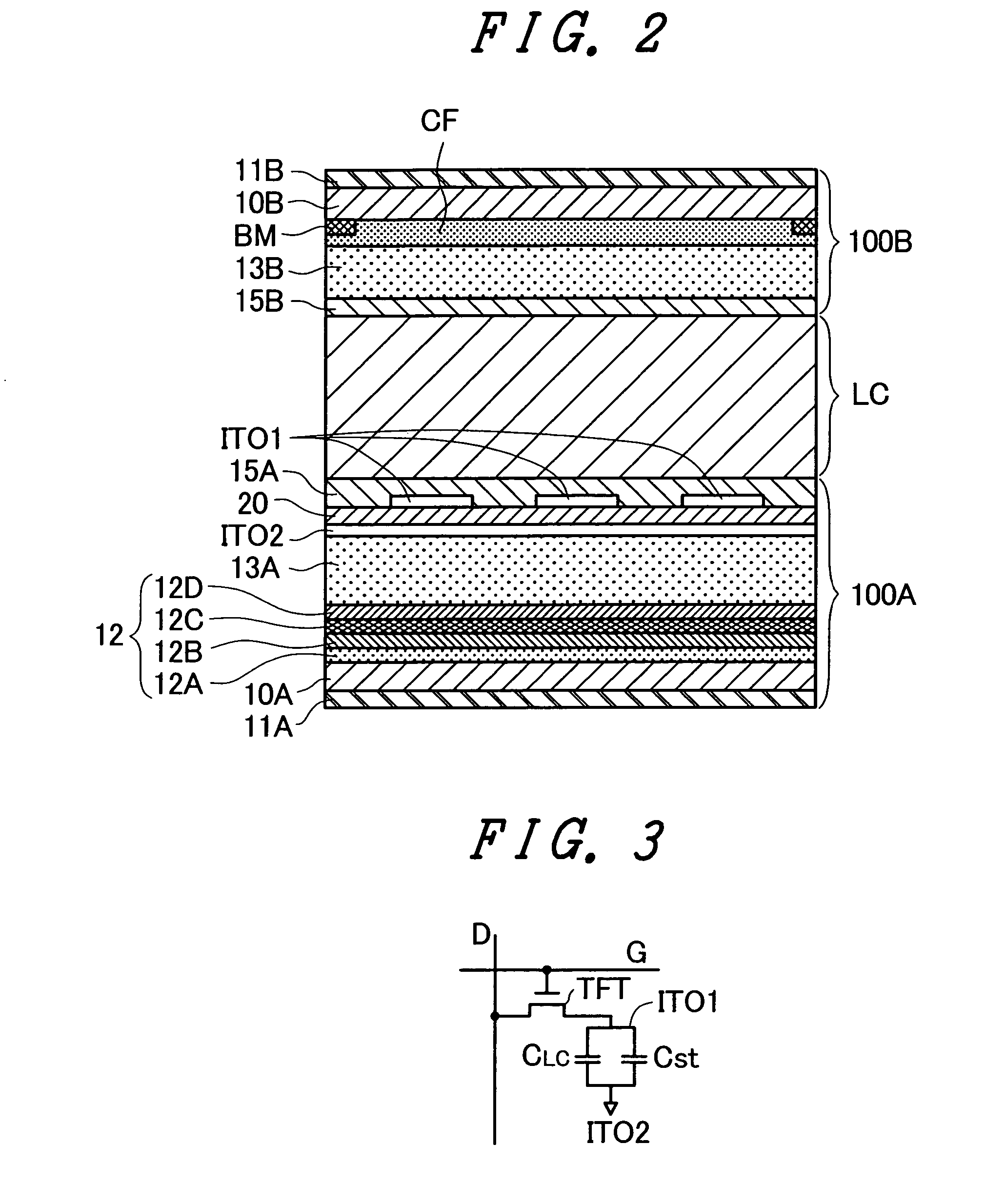
[0044]FIG. 2 is a cross sectional diagram showing the cross sectional configuration of a portion cut along a line A-A′ of FIG. 1. In the below, by referring to FIG. 2, the configuration of the liquid crystal display panel in this embodiment is described.

[0045] The liquid crystal display panel of this embodiment is an IPS liquid crystal display panel using a sheet-like opposing electrode, and as shown in FIG. 2, includes a transparent substrate (100B) and another transparent substrate (100A). These transparent substrates are disposed to ...


PUM


Abstract

A liquid crystal display device that includes a first substrate, a second substrate, and a liquid crystal material sandwiched between the first and second substrates. In the device, the first substrate includes an active element, a first insulation film formed above the active element, a first electrode formed above the first insulation film, a second insulation film formed above the first electrode, and a second electrode formed above the second insulation film. The second insulation film is a coating insulation film, the first insulation film has a first contact hole, the second insulation film is formed between the first and second electrodes, and inside of the first contact hole, the second insulation film formed inside of the first contact hole is formed with a second contact hole, the second electrode is a pixel electrode, the second electrode is electrically connected to the active element via the second contact hole, and a retention capacity is formed by the first and second electrodes and the second insulation film. The resulting liquid crystal display device of such a configuration causes no short circuit in a height-different portion between electrodes formed on both sides of an insulation film.

Description

[0001] The present application claims priority from Japanese application JP2005-312165 filed on Oct. 27, 2005, the content of which is hereby incorporated by reference into this application. BACKGROUND OF THE INVENTION [0002] The present invention relates to liquid crystal display devices and, more specifically, to a technology working effectively when applied to a substrate formed with an active element, e.g., thin film transistor, of a liquid crystal display panel. [0003] In an IPS (In-Plane Switching) (also referred to as horizontal-field-type) liquid crystal display panel, an electric field is generated between a pixel electrode and an opposing electrode to be parallel at least partially to a substrate. The electric field is used to drive a liquid crystal material, and light passing through a liquid crystal layer is modulated for image display. [0004] Such an IPS liquid crystal display panel is known for displaying images by modulating light passing through a liquid crystal laye...

Claims


Application Information

Patent Timeline
IPC IPC(8): G02F1/1333
CPCG02F1/133345G02F1/134363G02F1/136204G02F2201/124G02F1/1335G02F1/136
Inventor SONODA, DAISUKEOCHIAI, TAKAHIROKIMURA, YASUKAZUMAKI, MASAHIROMIYAZAWA, TOSHIO
Owner PANASONIC LIQUID CRYSTAL DISPLAY CO LTD
Why Eureka
Try Eureka