Apparatus and method for pressure bonding and method for manufacturing semiconductor device

a technology of semiconductor devices and apparatus, applied in auxillary welding devices, mechanical control devices, instruments, etc., can solve the problems of connection failure and more pressure than needed applied to the element group, so as to prevent excessive pressure from being applied, damage to an element such as a transistor included in the element group, the effect of preventing damag

Inactive Publication Date: 2007-05-17
SEMICON ENERGY LAB CO LTD
View PDF7 Cites 29 Cited by
  • Summary
  • Abstract
  • Description
  • Claims
  • Application Information

AI Technical Summary

Benefits of technology

[0016] When a substrate and an element group are pressure-bonded to each other, by performing the pressure bonding while monitoring a value and distribution of pressure applied to the element group and controlling the pressure applied at the time of the pressure bonding, the substrate and the element group can be sufficiently connected, excessive pressure is prevented from being applied to the element group, and damage to an element such as a transistor included in the element group can be prevented.

Problems solved by technology

However, there is a possibility that more pressure than needed is applied to the element group and an element such as a transistor is damaged, depending on a condition such as applied pressure or heat.
On the other hand, in a case where pressure to be applied at the time of pressure bonding is reduced so as to suppress damage to the element such as a transistor, there is a possibility that the substrate and the element group are not attached firmly enough to each other, leading to a connection failure.

Method used


Image

  • Apparatus and method for pressure bonding and method for manufacturing semiconductor device
  • Apparatus and method for pressure bonding and method for manufacturing semiconductor device
  • Apparatus and method for pressure bonding and method for manufacturing semiconductor device

Examples


embodiment mode 1

[0032] In this embodiment mode, an example of a pressure bonding apparatus and a pressure bonding method of the present invention will be described with reference to drawings. Specifically, the explanation will be made on a case where an element group is provided over a substrate by pressure bonding.

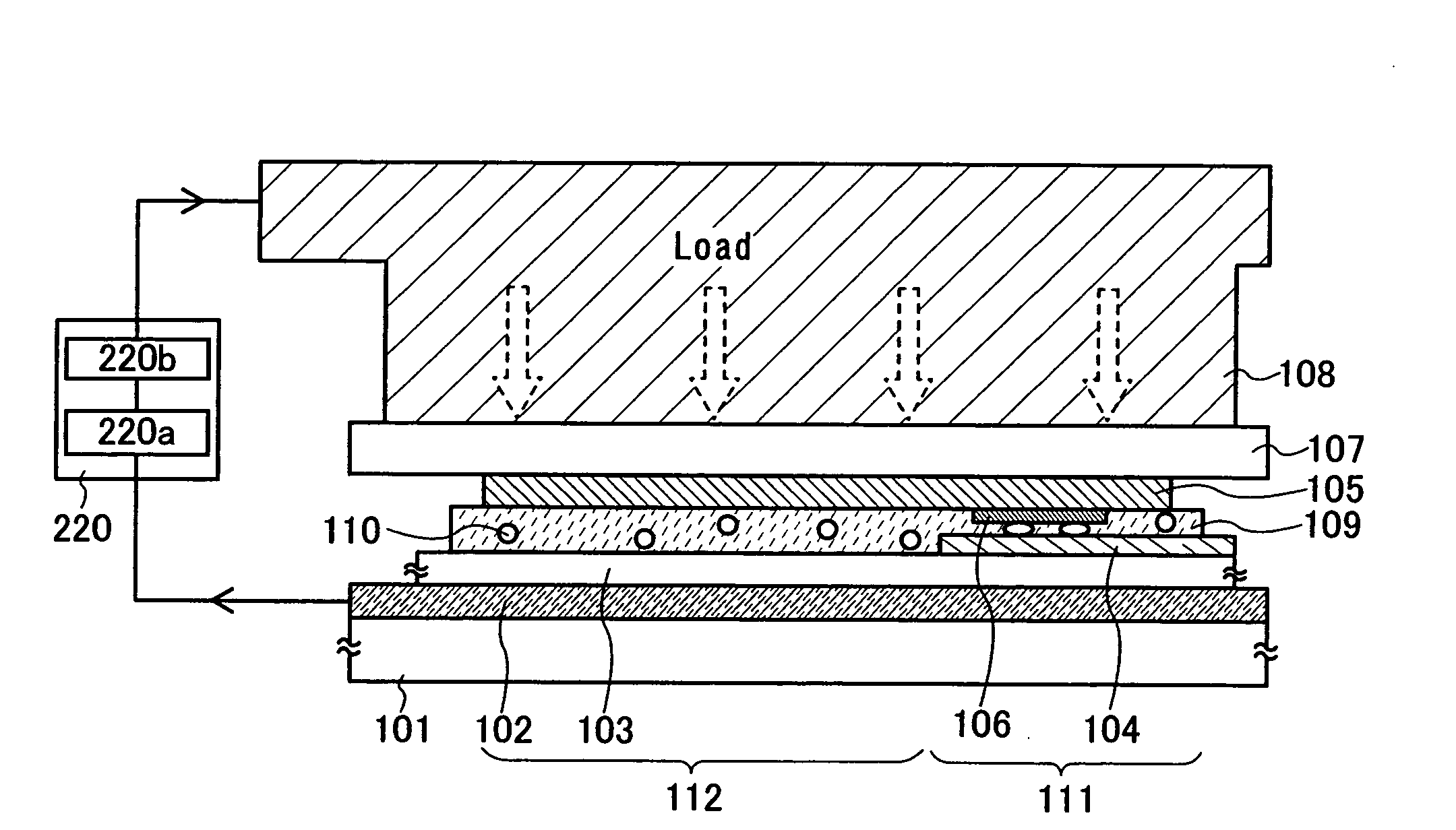
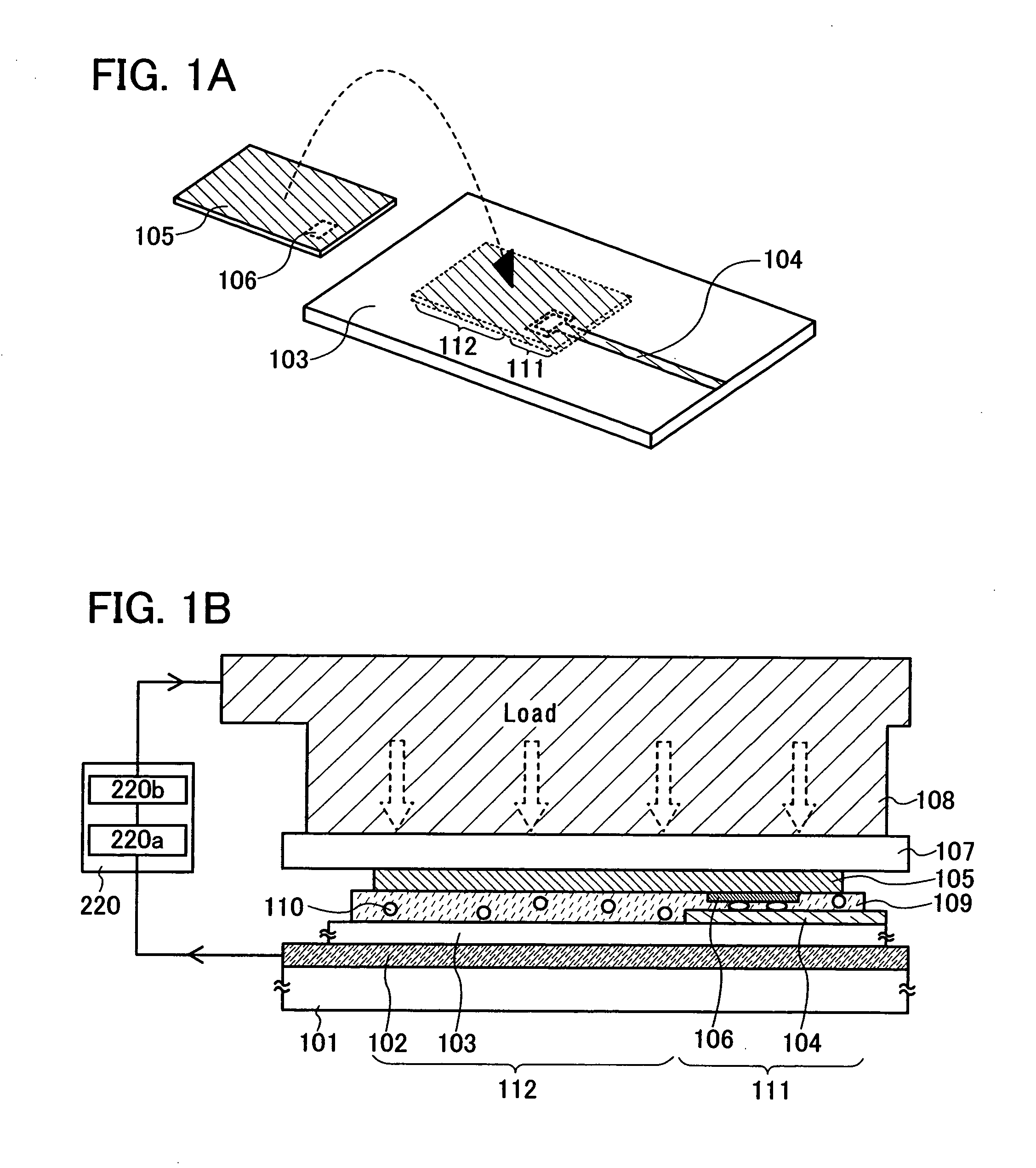
[0033]FIG. 1A shows a case where a conductive film 104 formed over a substrate 103 and an element group 105 are electrically connected to each other by pressure-bonding the element group 105 to the substrate 103. More specifically, FIG. 1A shows a case where the conductive film 104 formed over the substrate 103 and a conductive film 106 functioning as a bump formed over the element group 105 are pressure-bonded to each other via a material with adhesiveness such as an anisotropic conductive film (ACF) or an anisotropic conductive paste (ACP) so as to be electrically connected to each other. It is to be noted that “pressure bonding” herein means attaching two or more objects to each othe...

embodiment mode 2

[0051] In this embodiment mode, a different structure of a pressure bonding apparatus from the one explained in the above embodiment mode will be described with reference to drawings.

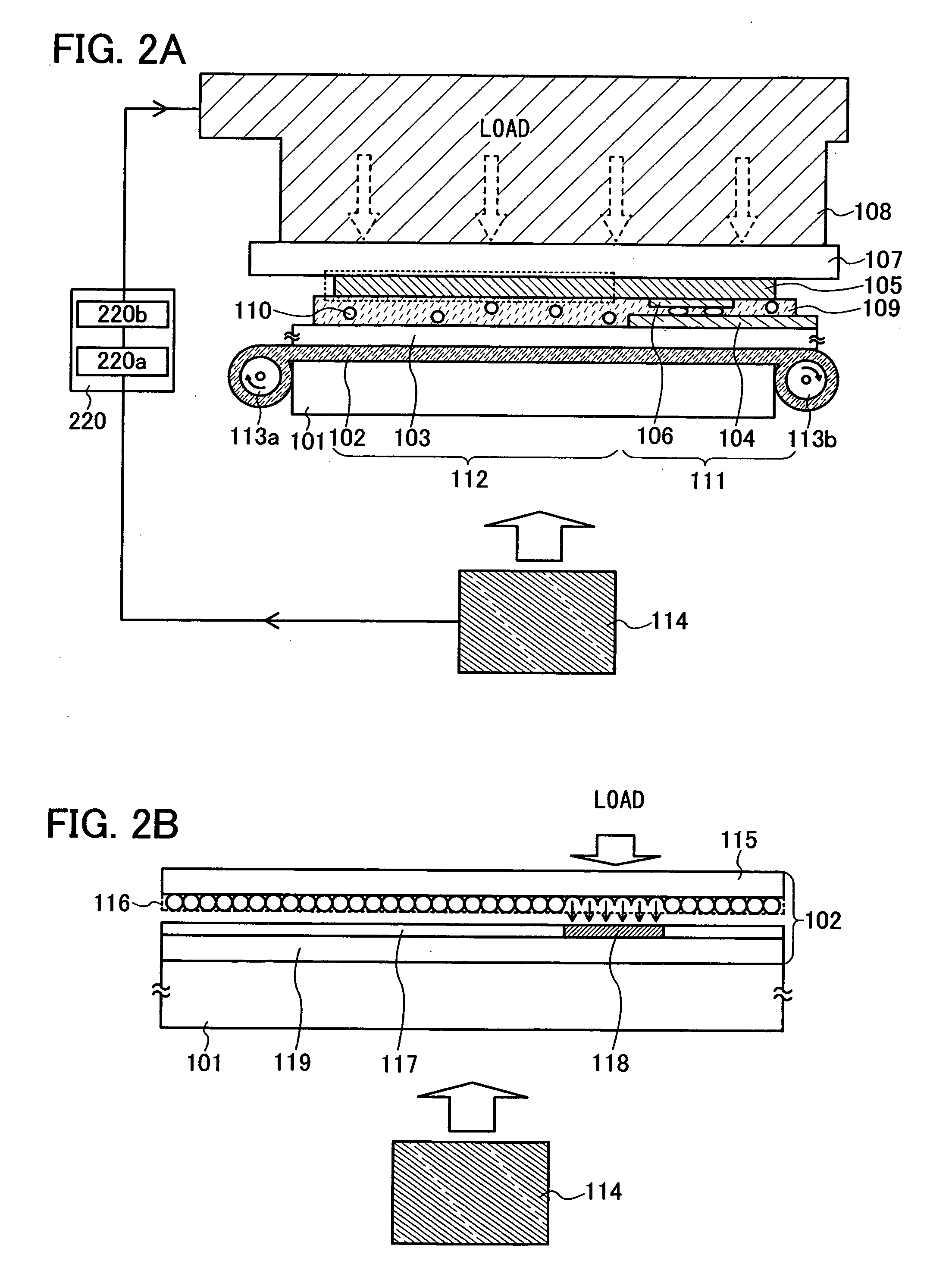
[0052] An example structure of a pressure bonding apparatus described in this embodiment mode is shown in FIGS. 2A and 2B. The pressure bonding apparatus shown in FIG. 2A includes at least a supporting substrate 101, a pressure detection film 102, a pressing table 107, a pressure-applying means 108, and an imaging device 114. Here, the pressure detection film 102 is provided over the supporting substrate 101, and a substrate 103 is placed over the pressure detection film 102. Then, in order to electrically connect a conductive film 104 formed over the substrate 103 to an element group 105, the substrate 103 and the element group 105 are pressure-bonded. Specifically, the substrate 103 and the element group 105 are attached to each other so that the conductive film 104 formed over the substrate 103 and ...

embodiment mode 3

[0064] In this embodiment mode, a different structure of a pressure bonding apparatus from the one explained in the above embodiment mode will be described with reference to drawings.

[0065] In the pressure bonding apparatus described in the above embodiment mode, an example of using a pressure-sensitive film as the pressure detection film is shown. However, the pressure detection film is acceptable as long as pressure applied to the element group which is placed above the pressure detection film can be detected.

[0066] As the pressure detection film 102 in FIG. 1B, a pressure sensor in which pressure-sensitive elements 121 which can detect a change in pressure are arranged in a matrix can be used (FIG. 3A). For example, by using pressure-sensitive elements which can convert a change in pressure into an electric signal, arranged in a matrix, a value and distribution of pressure applied to the element group when pressure-bonding the substrate and the element group can be detected.

[0...


PUM

PropertyMeasurementUnit
thicknessaaaaaaaaaa
thicknessaaaaaaaaaa
thicknessaaaaaaaaaa

Abstract

The substrate is placed over a pressure detection film, the element group is placed selectively over the substrate so that a conductive film functioning as an antenna formed over the substrate and a conductive film functioning as a bump formed over the element group overlap each other, the substrate and the element group are pressure-bonded to each other by applying pressure to the substrate and the element group so that the conductive film formed over the substrate and the conductive film functioning as a bump formed over the element group are electrically connected to each other, a value and distribution of pressure applied to the element group at the time of the pressure bonding are detected by the pressure detection film, and the pressure applied at the time of the pressure bonding is controlled, based on the detected pressure value and pressure distribution.

Description

BACKGROUND OF THE INVENTION [0001] 1. Field of the Invention [0002] The present invention relates to a pressure bonding apparatus and a pressure bonding method which are used in attaching an element to a substrate or the like, as well as a manufacturing method of a semiconductor device using the pressure bonding apparatus and pressure bonding method. [0003] 2. Description of the Related Art [0004] In recent years, individual recognition technology has received a lot of attention. For example, there is a technology to be used for production and management, in which information such as a history of the object is clarified by giving an ID (an individual recognition number) to an individual object. Above all, the development of semiconductor devices that can input and output data without contact has been advanced. As such semiconductor devices, for example, an RFID tag (Radio Frequency Identification) (also referred to as an ID tag, an IC tag, an IC chip, an RF tag (Radio Frequency), a ...

Claims


Application Information

Patent Timeline
Patent Type & Authority Applications(United States)
IPC IPC(8): B32B41/00B32B37/00B32B38/00
CPCB32B41/00B32B2309/12B32B2309/72B32B2519/02H01L21/67144H01L21/6835H01L24/75H01L24/83H01L2221/6835H01L2221/68368H01L2224/838H01L2924/01002H01L2924/01004H01L2924/01005H01L2924/01012H01L2924/01013H01L2924/01015H01L2924/01018H01L2924/01025H01L2924/01027H01L2924/01029H01L2924/0103H01L2924/01033H01L2924/0104H01L2924/01042H01L2924/01046H01L2924/01047H01L2924/01049H01L2924/01054H01L2924/0106H01L2924/01073H01L2924/01074H01L2924/01077H01L2924/01078H01L2924/01079H01L2924/01082H01L2924/04941H01L2924/04953H01L2924/0781H01L2924/14H01L2924/19043H01L2224/2919H01L2924/01006H01L2924/01023H01L2924/01024H01L2924/01041H01L2924/01044H01L2924/01045H01L2924/0105H01L2924/01067H01L2924/01068H01L2924/0107H01L2924/01076H01L2924/014H01L2924/0665H01L2924/00H01L2924/0132H01L2924/01014H01L2924/01028H01L2924/10253
Inventor TAKAHASHI, HIDEKAZUKUSUMOTO, NAOTO
Owner SEMICON ENERGY LAB CO LTD
Why Eureka
Try Eureka