Semiconductor processing system

a processing system and semiconductor technology, applied in the field of semiconductor processing system, can solve the problems of substantial reduction in throughput, difficulty in meeting requests, and unpractical level

Inactive Publication Date: 2007-05-17
ISHIZAWA SHIGERU +6
View PDF7 Cites 398 Cited by
  • Summary
  • Abstract
  • Description
  • Claims
  • Application Information

AI Technical Summary

Benefits of technology

[0013] Accordingly, an object of the present invention is to provide a semiconductor processing system that can easily incorporate either of additional processing apparatuses for performing a vacuum atmosphere process and an atmospheric pressure atmosphere process.

Problems solved by technology

However, the processing system shown in FIG. 14 has fixed structures, except for the three vacuum processing apparatuses 4A to 4, and thus is very difficult to comply with the request described above.
In this case, however, it takes a long time to perform pressure adjustment between chambers when wafers are transferred, thereby inevitably bringing about a substantial decrease in throughput, to an unpractical level.

Method used


Image

  • Semiconductor processing system
  • Semiconductor processing system
  • Semiconductor processing system

Examples


Embodiment Construction

[0048] Embodiments of the present invention will be described hereinafter with reference to the accompanying drawings. In the following description, the constituent elements having substantially the same function and arrangement are denoted by the same reference numerals, and a repetitive description will be made only when necessary.

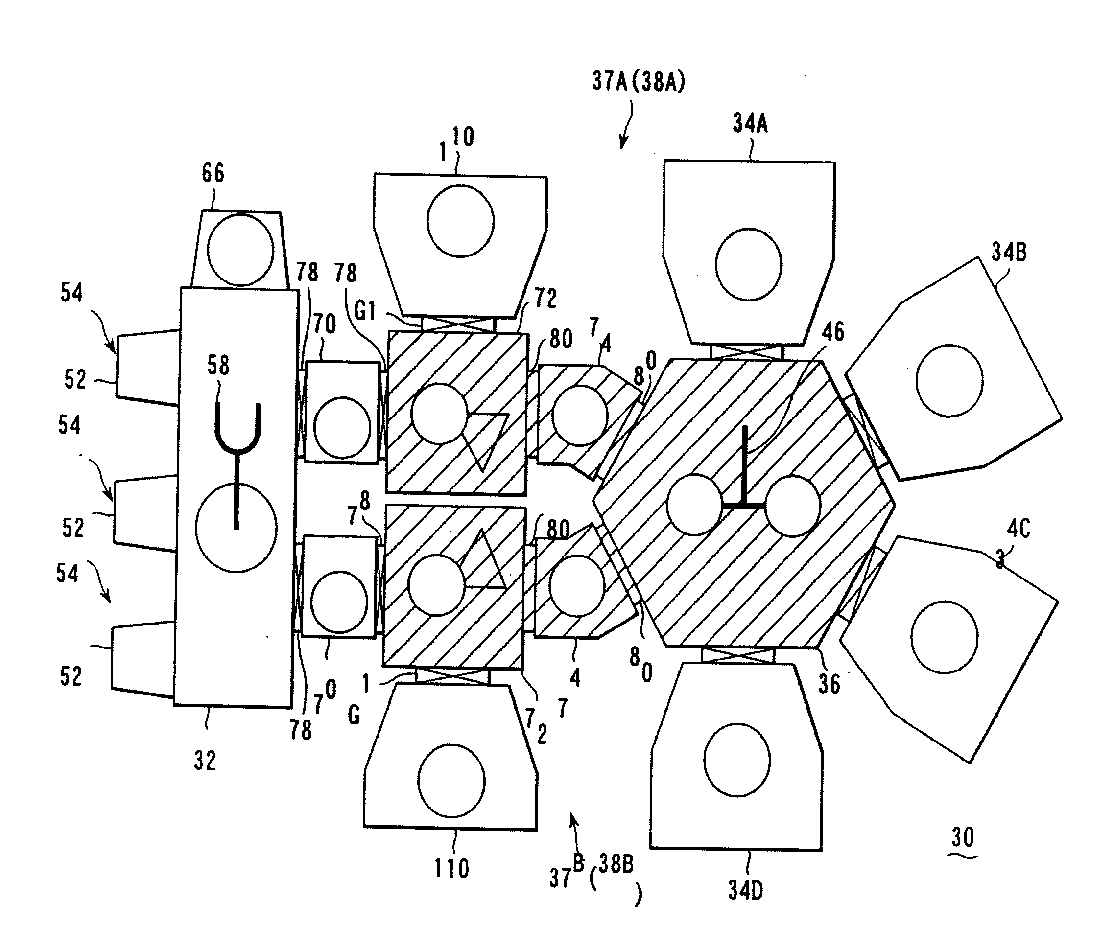
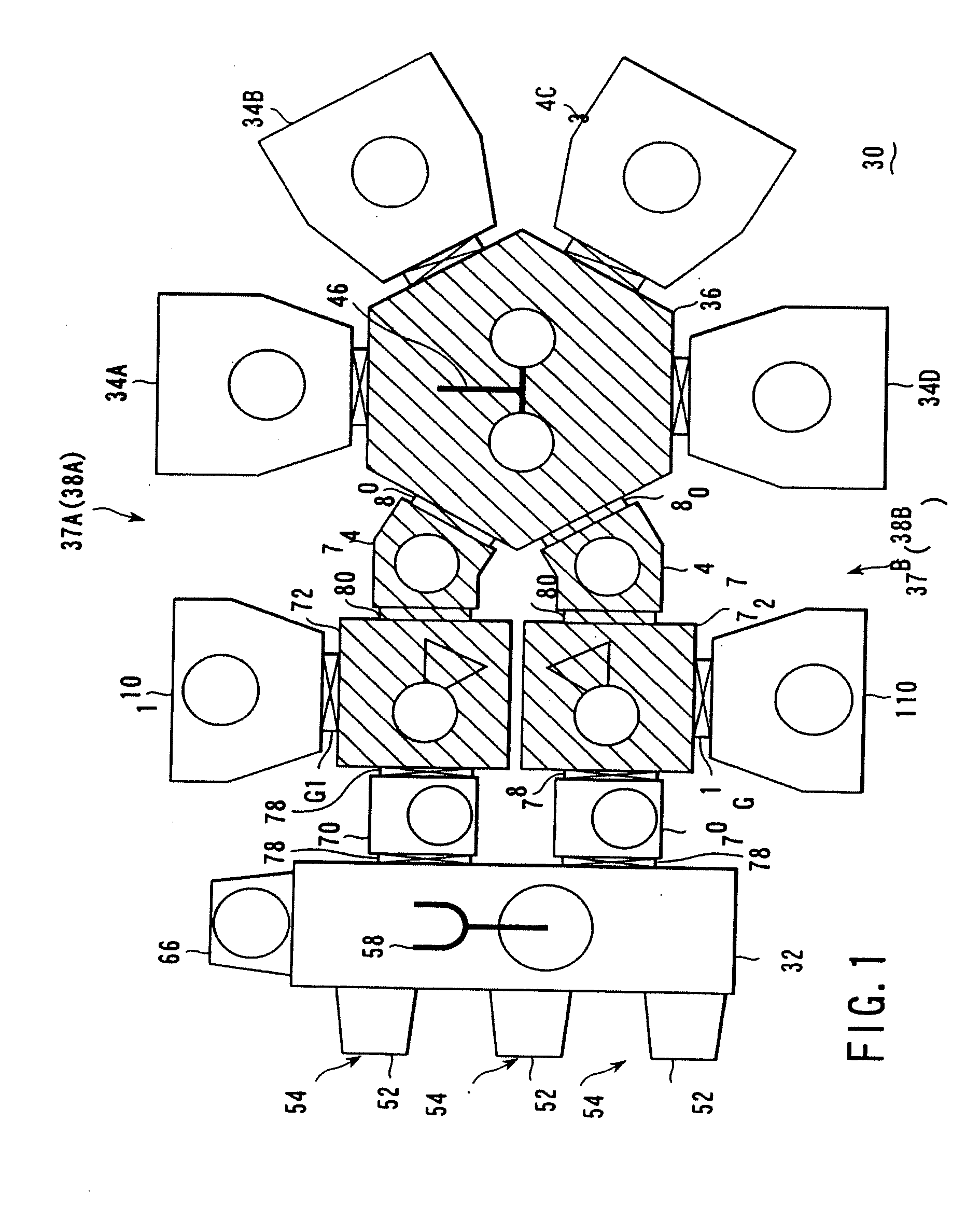
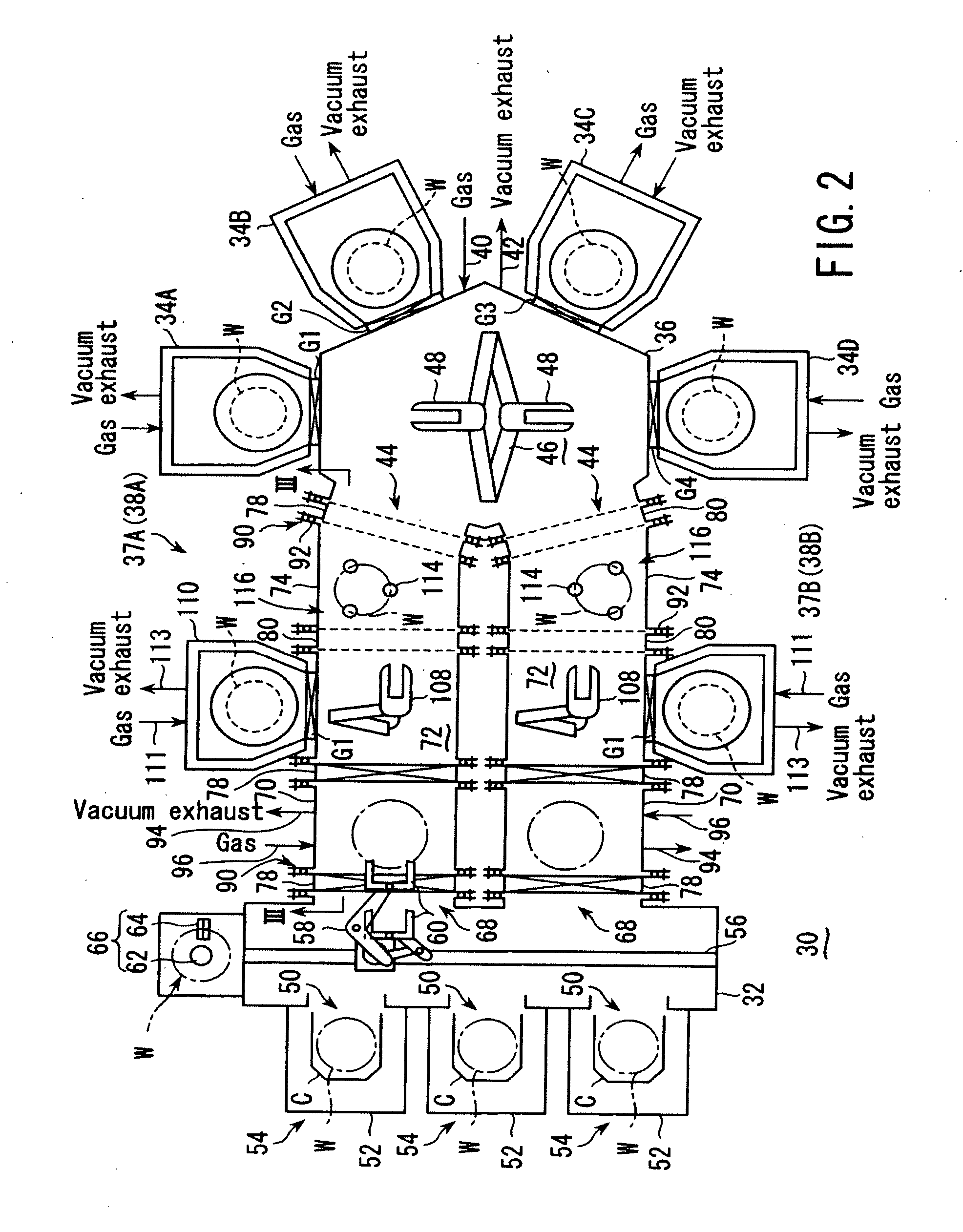
[0049]FIG. 1 is a schematic plan view showing one state of a semiconductor processing system according to an embodiment of the present invention. FIG. 2 is a plan view showing the processing system of FIG. 1 in detail. FIG. 3 is an enlarged sectional view taken along line III-III in FIG. 2. The shaded portions in FIG. 1 denote portions that are kept in continuous vacuum when the system operates. The shaded portions in the plan views shown in FIGS. 7, 10, 12, and 13 denote the same.

[0050] As shown in FIGS. 1 and 2, the processing system 30 includes an entrance transfer chamber 32 with an atmospheric pressure atmosphere, into which a target substrate, su...


PUM

PropertyMeasurementUnit
timeaaaaaaaaaa
timeaaaaaaaaaa
timeaaaaaaaaaa

Abstract

A semiconductor processing system includes an intermediate structure disposed between an atmospheric pressure entrance transfer chamber and a vacuum common transfer chamber. The intermediate structure includes a transfer passage for a target substrate to pass therein. The transfer passage includes a first buffer chamber a middle transfer chamber and a second buffer chamber detachably connected. An additional processing apparatus is detachably connected to the middle transfer chamber. The intermediate structure is selectively arranged in first or second state. In the first state, the additional processing apparatus performs a vacuum process, while the first buffer chamber is a load-lock chamber. In the second state, the additional processing apparatus performs an atmospheric pressure process, while the second buffer chamber is a load-lock chamber.

Description

CROSS-REFERENCE TO RELATED APPLICATIONS [0001] This application is a Continuation of and claims the benefit of priority under 35 U.S.C. §120 from U.S. Ser. No. 10 / 486,511, filed on Feb. 12, 2004, which is a national stage of international filing PCT / JP02 / 07817 filed Jul. 31, 2002. This application also claims the benefit of priority under 35 U.S.C. §119 from Japanese Patent Application No. 2001-246088, filed Aug. 14, 2001, the entire contents of each which is incorporated herein by reference.TECHNICAL FIELD [0002] The present invention relates to a semiconductor processing system having a plurality of vacuum processing apparatuses for performing predetermined processes on a target substrate, such as a semi-conductor wafer. The term “semiconductor process” used herein includes various kinds of processes which are performed to manufacture a semiconductor device or a structure having wiring layers, electrodes, and the like to be connected to a semiconductor device, on a target substrat...

Claims


Application Information

Patent Timeline
Patent Type & Authority Applications(United States)
IPC IPC(8): C23F1/00H01L21/306C23C16/00B65G49/00H01L21/00H01L21/677
CPCH01L21/67109H01L21/67115H01L21/67184H01L21/67201H01L21/67751
Inventor ISHIZAWA, SHIGERUSAEKI, HIROAKITAMURA, YOSHIMITSUHOSAKA, SHIGETOSHIITOH, MASAHIDETAHARA, KAZUSHIKODASHIMA, YASUSHI
Owner ISHIZAWA SHIGERU
Why Eureka
Try Eureka