Packaging structure of mini SD memory card

Inactive Publication Date: 2007-05-17
SUN LIGHT ELECTRONICS TECH
View PDF8 Cites 21 Cited by
  • Summary
  • Abstract
  • Description
  • Claims
  • Application Information

AI Technical Summary

Benefits of technology

[0006] It is an object of the present invention to provide an improved packaging structure of a type of memory card. More particularly, the present invention relates to an improved packaging structure of mini SD memory card. The present invent provide an improved design that has enough space within the mini SD memory card package so

Problems solved by technology

Thus, the manufacturing cost of the package of the memory card is increased.
Furthermore, those expansive IC devices are not reliable, an

Method used


Image

  • Packaging structure of mini SD memory card
  • Packaging structure of mini SD memory card
  • Packaging structure of mini SD memory card

Examples


Embodiment Construction

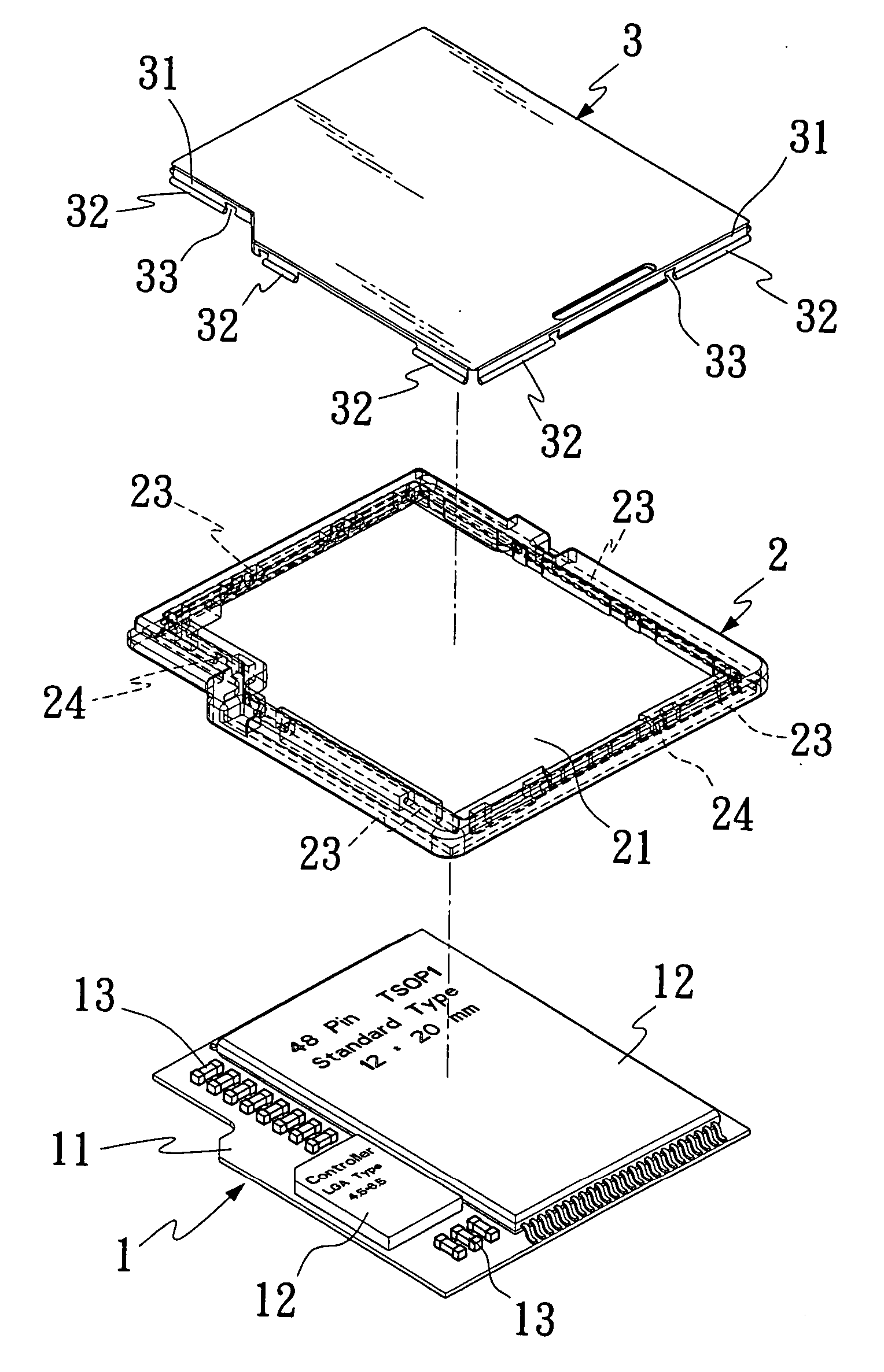
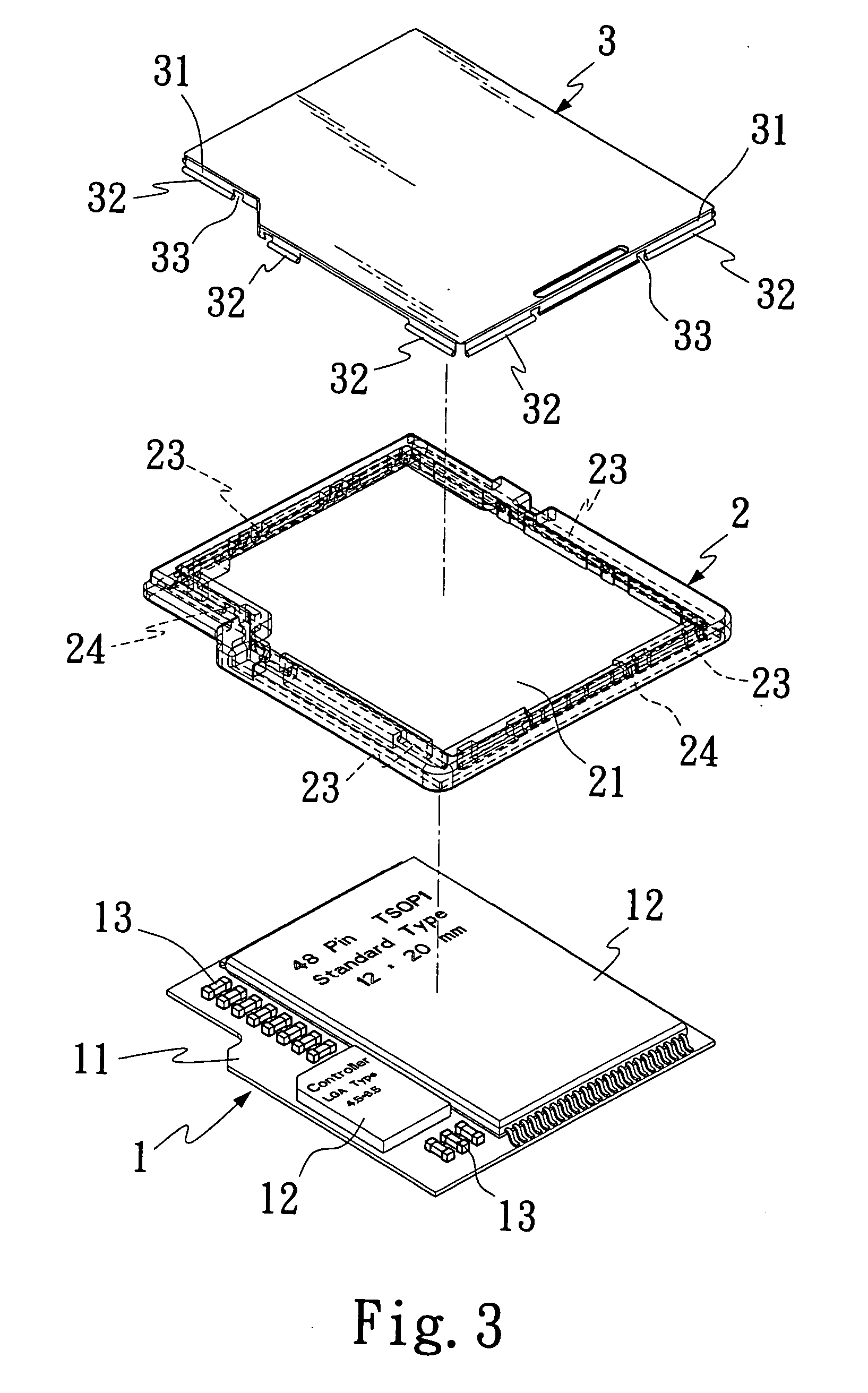
[0018] Refer to FIG. 3 and FIG. 4, the present invention provides an improved packaging structure of mini SD memory card, the improved structure comprises a substrate 1, a frame 2 and a metal cover 3. Wherein the substrate 1, as shown in FIG. 3 and FIG. 4, is a circuit board consisting required circuits formed on its platform. An inner platform 11 comprising various type of integrated circuit (IC) devices 12 that are required by a memory card, such as the control chip device and flash IC chip, as well as other passive devices 13. A plurality of pins 15 qualified for utilizing in the mini SD memory card are formed in an outer platform 14. The pins 15 can electrical connected to other electrical products rapidly, such as a carryable memory device, cell phone digital camera and reading memory device.

[0019] The frame 2, as shown in FIG. 3 and FIG. 4, is a square plastic frame for locating the substrate 1 and is utilized to protect the IC devices 12 and the passive devices 13. The metal...


PUM


Abstract

The present invention provides an improved packaging structure of a memory card, such as mini SD memory card. The packaging structure comprises a substrate having a plurality of integrated circuit devices and passive devices located therein, and a metal cover having an insulating layer formed on a top portion of the metal cover. A plurality of protruding plates bending downward are formed around a circumferential area of the metal cover, and a roll-shaped fixing part is formed at a bottom portion of a particular protruding plate. The roll-shaped fixing part and the protruding plates are utilized to engage the frame with the metal cover to form a sealed structure so that the frame covers all the protruding plates and the roller-shaped fixing part of the metal cover. The integrated circuit devices and the passive devices are located within the space of the frame to form a mini SD memory card package.

Description

BACKGROUND OF THE INVENTION [0001] 1. Field of Invention [0002] The present invention relates generally to an improved structure of memory card package. More particularly, the present invention relates to an improved design of a package structure of mini SD memory card. [0003] 2. Description of the Related Art [0004] The conventional package structure of mini SD memory card is showed in FIG. 1 and FIG. 2. The package structure comprises a plastic cover 10 covered a memory substrate 20. The plastic cover 10 comprises a L-shaped upper cover 101 and a bottom cover 102. When the upper cover 101 and the bottom cover 102 are integrated together, a space 103 is form in between. Variety of integrated circuit (IC) devices and passive devices are formed on a top surface of a circuit of the memory substrate 20 (including flash IC). A plurality of golden fingers are formed on a back surface of the circuit and electrically connected to other electrical products. The memory substrate 20 is then p...

Claims


Application Information

Patent Timeline
IPC IPC(8): G06K19/06H05K1/14
CPCH05K5/026
Inventor LIU, CHIN-CHUNLIU, SHIH-TUNG
Owner SUN LIGHT ELECTRONICS TECH
Why Eureka
Try Eureka