
Stacked CMOS current mirror using MOSFETs having different threshold voltages

Inactive Publication Date: 2007-05-17
SAMSUNG ELECTRONICS CO LTD
View PDF0 Cites 6 Cited by
  • Summary
  • Abstract
  • Description
  • Claims
  • Application Information

AI Technical Summary

Benefits of technology

[0012] The present invention provides a stacked CMOS current mirror which can minimize the minimum saturation operating voltages of the MOSFETs and sufficiently secure an output voltage swing range by using MOSFETs having different threshold voltages for improving the output resistance of the current mirror.

Problems solved by technology

However, it is difficult to implement an integrated circuit which operates at low voltage.
In particular, it is difficult to implement a current mirror for an MOS analog circuit that operates at low voltage and has an improved characteristic.
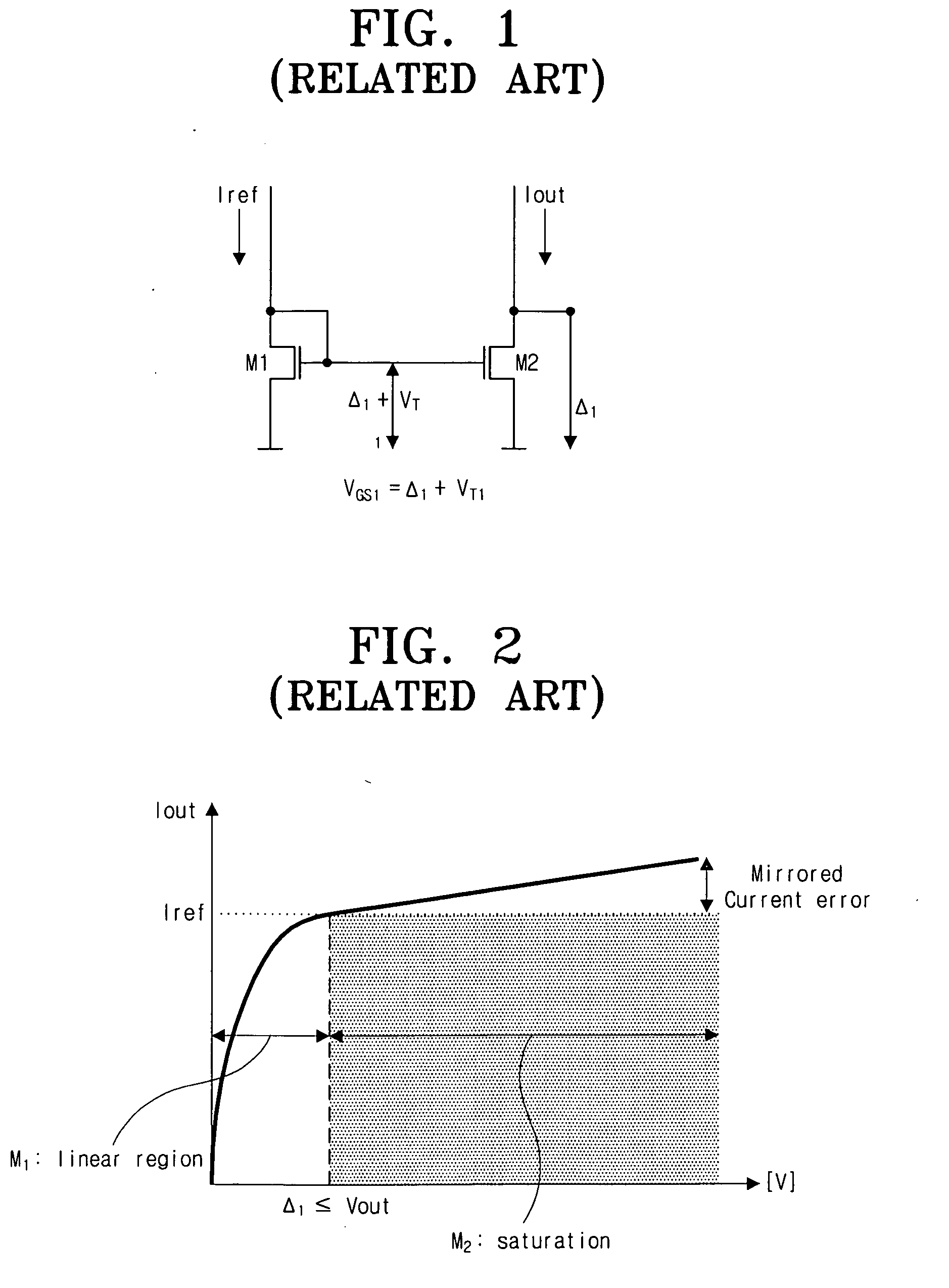
In the conventional current mirror, however, both the minimization of the minimum saturation operating voltage and the securing of the output voltage swing range are not satisfied.
Referring to FIG. 2, the conventional CMOS current mirror does not satisfy the securing requirement of the output voltage swing range because an error in that the reference current Iref does not coincide with the current-mirrored current occurs due to the small output resistance of the current mirror.

Method used


Image

  • Stacked CMOS current mirror using MOSFETs having different threshold voltages
  • Stacked CMOS current mirror using MOSFETs having different threshold voltages
  • Stacked CMOS current mirror using MOSFETs having different threshold voltages

Examples


Embodiment Construction

[0023] Certain exemplary embodiments of the present invention will be described in greater detail with reference to the accompanying drawings.

[0024] In the following description, same drawing reference numerals are used for the same elements even in different drawings. The matters defined in the description such as a detailed construction and elements are nothing but the ones provided to assist in a comprehensive understanding of the invention. Thus, it is apparent that the present invention can be carried out without those defined matters. Also, well-known functions or constructions are not described in detail since they would obscure the invention in unnecessary detail.

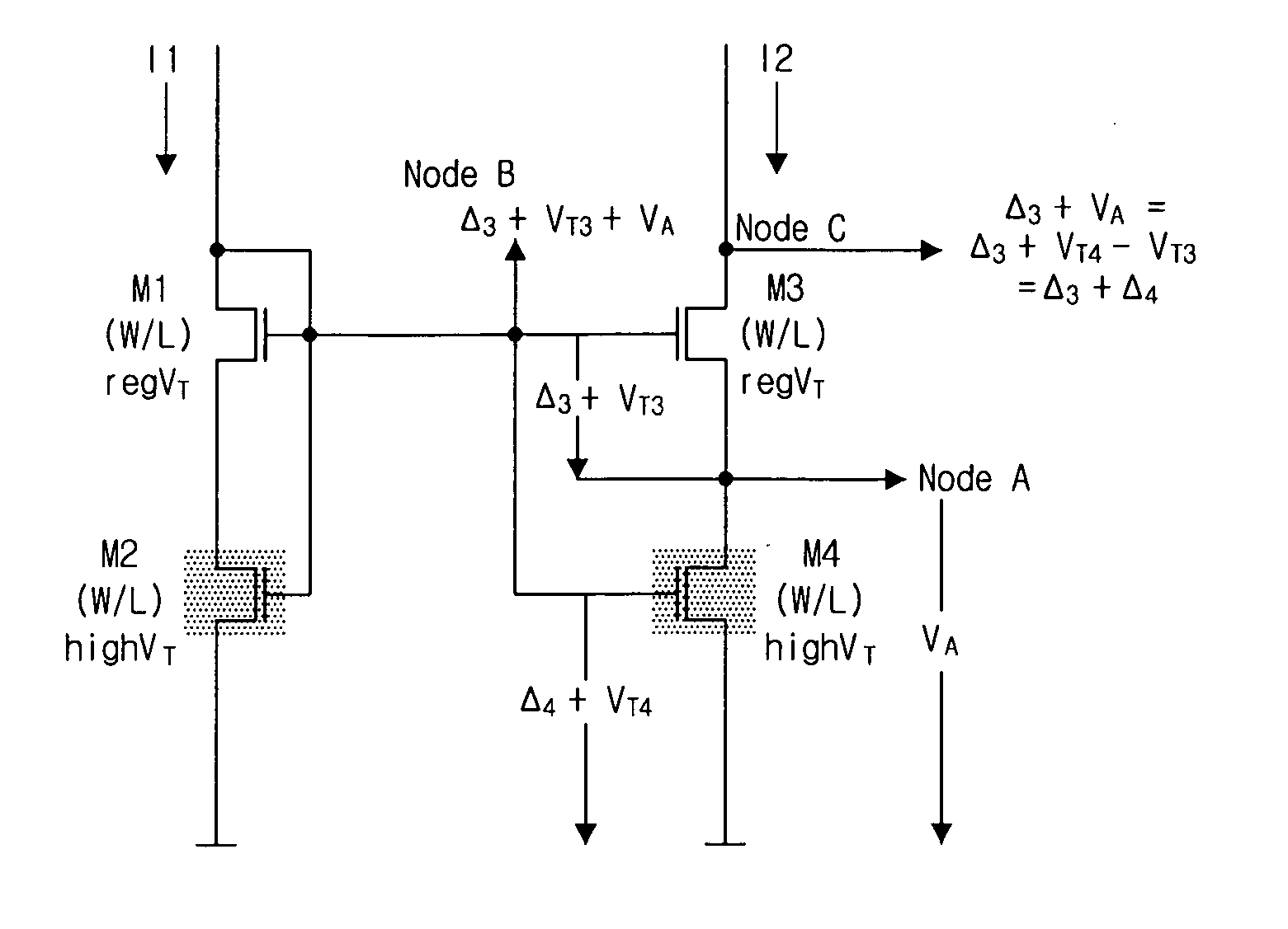
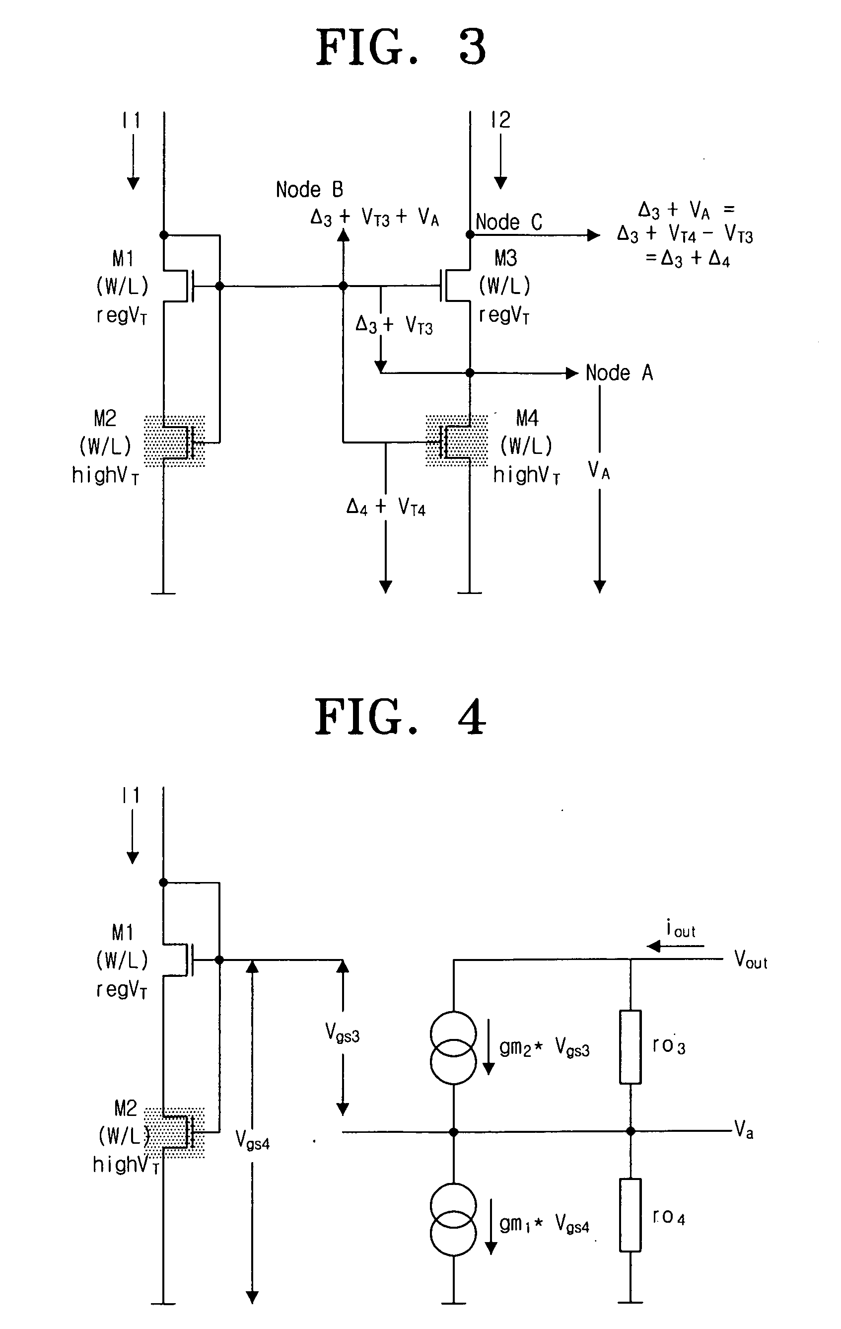
[0025]FIG. 3 is a circuit diagram of a CMOS current mirror according to an exemplary embodiment of the present invention.

[0026] Referring to FIG. 3, the stacked CMOS current mirror according to the present invention includes four MOSFETs M1, M2, M3 and M4.

[0027] The MOSFET M1 has-a drain and a gate which are con...


PUM


Abstract

A stacked CMOS current mirror using metal oxide semiconductor field effect transistors (MOSFETs) having different threshold voltages is disclosed. The stacked CMOS current mirror includes a first MOSFET having a drain and a gate which are connected to an input current terminal, a second MOSFET having a drain connected to a source of the first MOSFET, a gate connected to the drain and the gate of the first MOSFET, and a source connected to ground, a third MOSFET having a drain connected to an output current terminal and a gate connected to the drain and the gate of the first MOSFET and the gate of the second MOSFET, and a fourth MOSFET having a drain connected to a source of the third MOSFET, a gate connected to the drain and the gate of the first MOSFET, the gate of the second MOSFET and the gate of the third MOSFET, and a source connected to the ground.

Description

CROSS-REFERENCE TO RELATED APPLICATION [0001] This is a Continuation-in-Part of U.S. application Ser. No. 11 / 354,944 filed Feb. 16, 2006, the entire content of which is incorporated herein by reference. This application claims priority from Korean Patent Application 10-2006-0047565 filed on May 26, 2006 and Korean Patent Application No. 10-2005-0013260 filed on Feb. 17, 2005, the entire contents of which are incorporated herein by reference.BACKGROUND OF THE INVENTION [0002] 1. Field of the Invention [0003] The invention relates to a stacked complementary metal oxide semiconductor (CMOS) current mirror. More particularly, the present invention relates to a stacked CMOS current mirror capable of sufficiently securing an output voltage swing range by decreasing the minimum saturation output operating voltage of the current mirror using metal oxide semiconductor field effect transistors (MOSFETs). [0004] 2. Description of the Related Art [0005] Recently, as the integration of integrate...

Claims


Application Information

Patent Timeline
IPC IPC(8): G05F1/10
CPCG05F3/262
Inventor KOH, JEONG-WOOKSUH, CHUN-DEOK
Owner SAMSUNG ELECTRONICS CO LTD
Learn More