
Current source circuit and differential amplifier

a current source circuit and amplifier technology, applied in the direction of differential amplifiers, amplifiers with semiconductor devices/discharge tubes, amplifiers with semiconductor devices only, etc., can solve the problems of difficult to increase reduce the gain of the differential amplifier, etc., and achieve easy supply of current sources and high output resistance

Inactive Publication Date: 2007-11-13
RENESAS ELECTRONICS CORP
View PDF1 Cites 4 Cited by
  • Summary
  • Abstract
  • Description
  • Claims
  • Application Information

AI Technical Summary

Benefits of technology

The present invention provides a circuit configuration that can easily provide a current source with a high output resistance, even through the output resistance of an MOS transistor is reduced due to short channel effect. This is achieved by adding a negative resistance generation block in parallel to the current source, which increases the output resistance of the current source circuit. This circuit configuration can also be used in a differential amplifier to increase the gain of the amplifier by controlling the output resistance and negative resistance of the amplifier to be substantially the same.

Problems solved by technology

Thus the reduced output resistance of the differential amplifier results in reduced gain of the differential amplifier.
However, the differential amplifier using cascode connection fails to prevent the reduction of an output resistance caused by short channel effect, thus making it difficult to increase the gain of the differential amplifier.

Method used


Image

  • Current source circuit and differential amplifier
  • Current source circuit and differential amplifier
  • Current source circuit and differential amplifier

Examples


first preferred embodiment

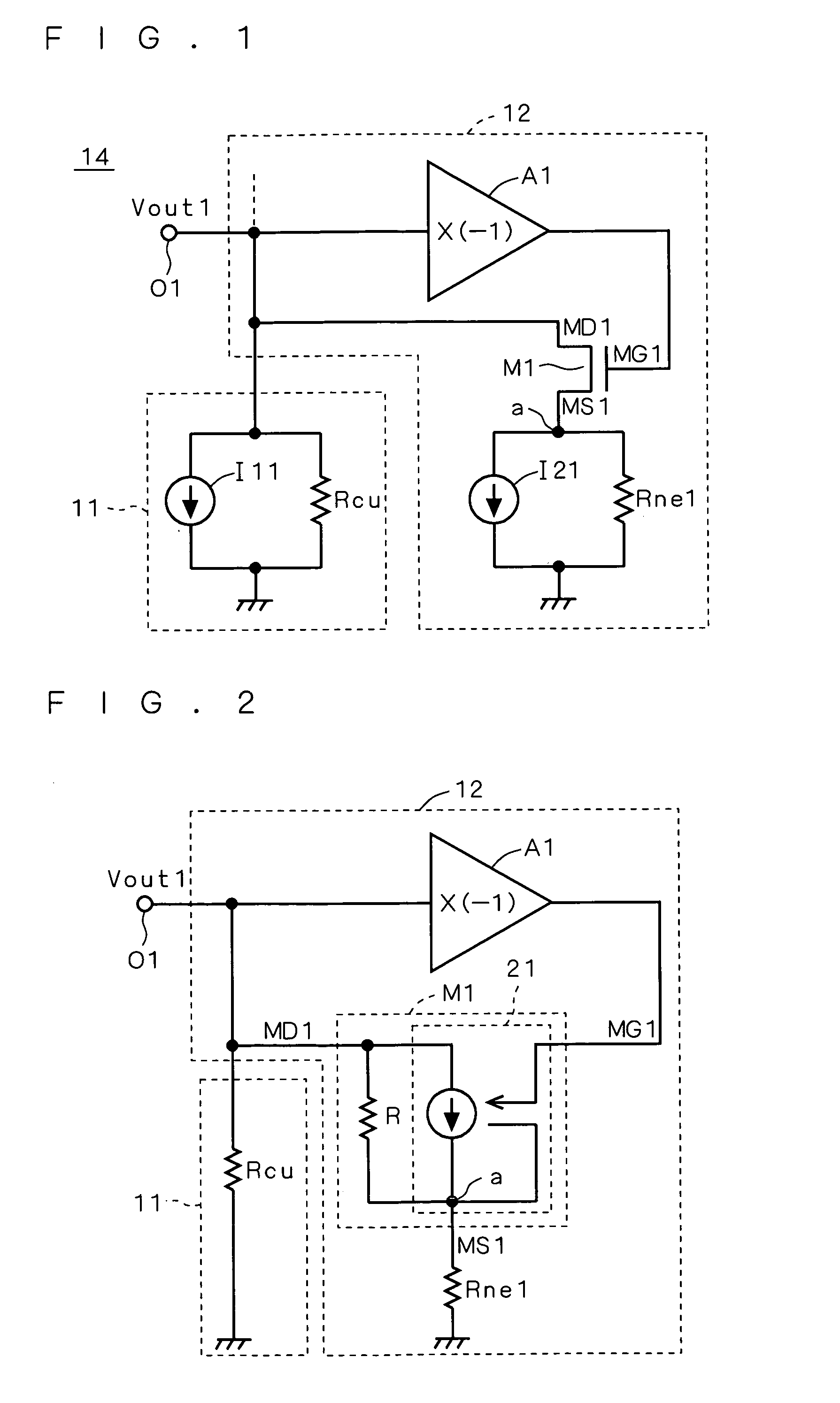
[0024]FIG. 1 is a circuit diagram showing the configuration of a current source circuit 14 according to a first preferred embodiment of the present invention. The current source circuit 14 has a parallel connection of a current source block (current source) 11 and a negative resistance generation block 12.

[0025]The negative resistance generation block 12 is configured as follows. The input of an amplifier A1 (inverting amplifier) providing a voltage gain of −1 is connected to an output terminal O1 (first differential output terminal). The output of the amplifier A1 is connected to a voltage-controlled terminal MG1 of an MOS transistor (voltage-controlled current source) M1. The MOS transistor M1 has a terminal MD1 (current input terminal) connected to the output terminal O1, and a terminal MS1 (current output terminal) connected at a node a to one end of a resistor (internal resistor) Rne1 (in the following, the resistance of the resistor Rne1 will also be identified as Rne1). Anoth...

second preferred embodiment

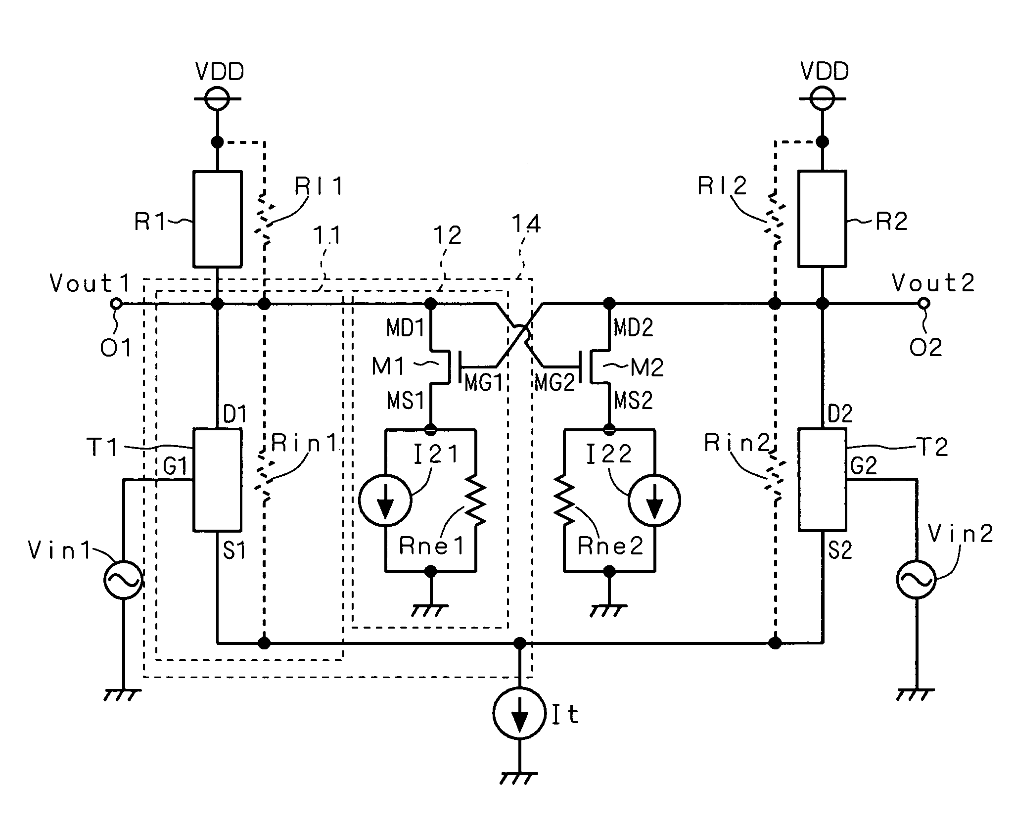
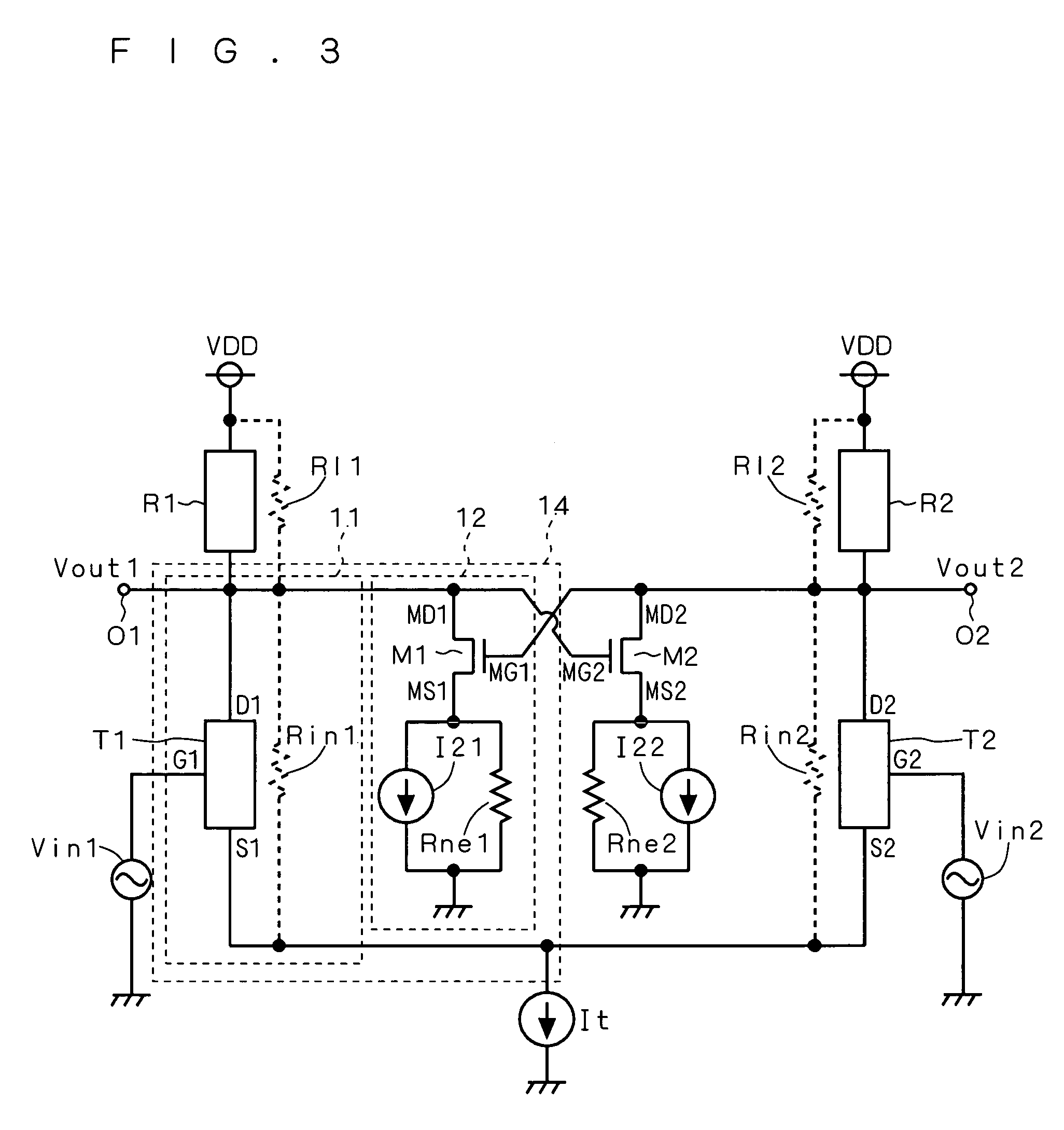
[0038]FIG. 3 is a circuit diagram showing the configuration of a differential amplifier according to a second preferred embodiment of the present invention. The differential amplifier of the second preferred embodiment employs the current source circuit 14 of the first preferred embodiment. In FIG. 3, respective resistors R11 and R12 of loads R1 and R2, and respective resistors Rin1 and Rin2 of voltage-controlled current sources T1 and T2 are represented by dotted lines. In the following, the respective resistances of the resistors R11, R12, Rin1 and Rin2 will be identified by the same reference numerals.

[0039]The load R1 has one end connected to a power source voltage VDD, and another end connected to the output terminal (first differential output terminal) O1. The voltage-controlled current source T1 has a terminal D1 connected to the output terminal O1, and a terminal S1 connected to one end of a constant current source It. Another end of the constant current source It is grounde...

third preferred embodiment

[0052]FIG. 5 is a circuit diagram showing the configuration of a differential amplifier according to a third preferred embodiment of the present invention. In the third preferred embodiment, the differential amplifier of the second preferred embodiment is more specifically configured using MOS transistors.

[0053]A PMOS transistor Mp1 has a source connected to the power source voltage VDD. The substrate terminal of the PMOS transistor Mp1 is also connected to the power source voltage VDD. The PMOS transistor Mp1 has a drain connected to the output terminal O1. An NMOS transistor Mn1 has a drain connected to the output terminal O1, a source connected to one end of the constant current source It, and a substrate terminal connected to the source.

[0054]Another end of the constant current source It is grounded. The gate of the NMOS transistor Mn1 is connected to one end of the voltage source Vin1. Another end of the voltage source Vin1 is grounded.

[0055]An NMOS transistor Mn3 has a drain c...


PUM


Abstract

A current source block and a negative resistance generation block are connected in parallel. The negative resistance generation block generates a negative resistance in response to the minute variations of an output voltage. Thus the output resistance of a current source circuit is given by the combined resistance of the negative resistance and the resistance of a resistor in the current source block connected in parallel. The resistance of the resistor in the current source block and the negative resistance are controlled to be substantially the same to thereby increase the output resistance of the current source circuit. The current source circuit serves to increase an output resistance when viewed from an differential output terminal. As a result, use of this current source circuit realizes a differential amplifier providing a high gain.

Description

BACKGROUND OF THE INVENTION[0001]1. Field of the Invention[0002]The present invention relates to a current source circuit and a differential amplifier, and more particularly to a current source circuit realizing increase of an output resistance and a differential amplifier using this current source circuit.[0003]2. Description of the Background Art[0004]A current source providing a high output resistance (rds) is ideally suited in a semiconductor integrated circuit. However, a recent trend for downsizing process makes a shorter channel length of an MOS transistor. The output resistance of a current source including an MOS transistor is reduced accordingly by short channel effect.[0005]In a differential amplifier using such a current source, the output resistance of the differential amplifier is reduced when viewed from a differential output terminal providing a differential signal. The differential amplifier provides a gain that is in proportion to the output resistance of the diffe...

Claims


Application Information

Patent Timeline
Patent Type & Authority Patents(United States)
IPC IPC(8): H03F3/45
CPCH03F3/45183H03F2203/45644
Inventor KAMAKURA, MASAOMIMIKI, TAKAHIRO
Owner RENESAS ELECTRONICS CORP
Learn More