High voltage gain topology for analog circuits in short channel technologies

a short channel, high-voltage gain technology, applied in the field of short channel length mos transistors, can solve the problems of mos transistors that are difficult to meet the requirements of short channel voltage, the voltage required to deplete the channel is reduced, and the behavior of mos transistors is different from conventional models, so as to achieve better noise immunity, lower leakage, and higher output resistance

Inactive Publication Date: 2006-10-12
AVAGO TECH INT SALES PTE LTD
View PDF11 Cites 4 Cited by
  • Summary
  • Abstract
  • Description
  • Claims
  • Application Information

AI Technical Summary

Benefits of technology

[0008] In another aspect of the invention, the stacked MOS configuration is used to replace an equivalent single MOS transistor block in a short channel length analog block. In an embodiment, the stacked MOS configuration provides a higher threshold voltage than the single MOS transistor block, thereby achieving lower leakage and better noise immunity. In another embodiment, the stacked MOS configuration results in a higher output resistance than the single MOS transistor, thereby providing higher intrinsic gain and lower gain variation due to temperature.

Problems solved by technology

As transistor geometries shrink, however, short-channel effects cause a variety of shifts in the behavior of MOS transistors away from conventional models.
In short-channel technology, however, this solution works adversely.
In fact, an increase in the channel length of a short-channel MOS results in a decrease in the voltage required to deplete the channel, lowering the channel resistance and, consequently, the intrinsic gain of the MOS.

Method used


Image

  • High voltage gain topology for analog circuits in short channel technologies
  • High voltage gain topology for analog circuits in short channel technologies
  • High voltage gain topology for analog circuits in short channel technologies

Examples


Embodiment Construction

Intrinsic Gain of a MOS Transistor

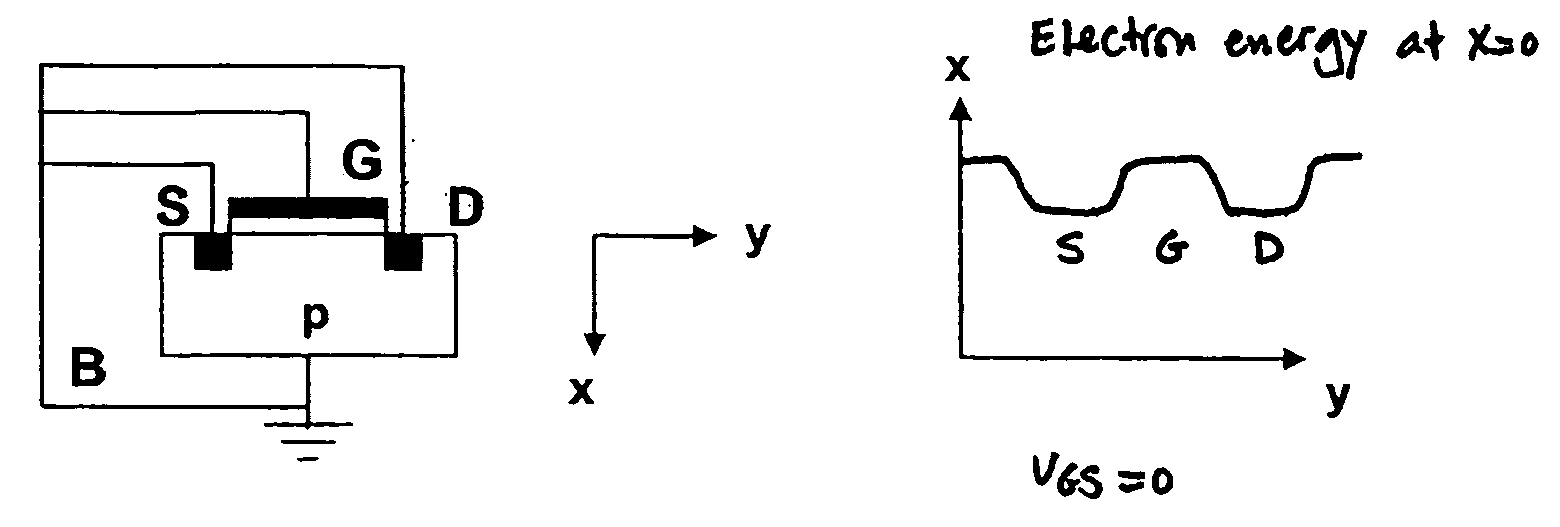
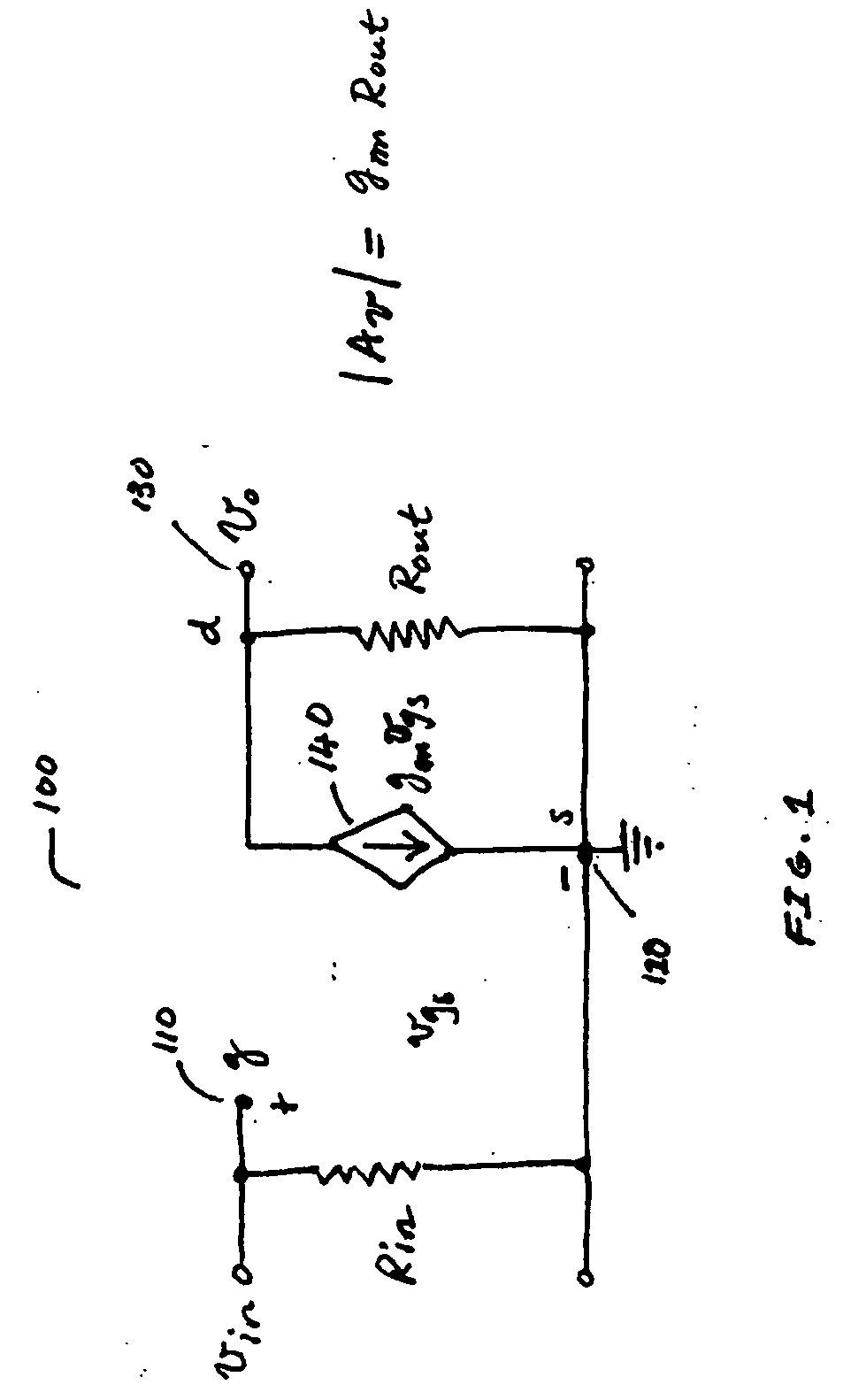
[0018]FIG. 1 illustrates a small-signal model representation of a MOS transistor. The representation of FIG. 1 shows a circuit 100 having an input resistance Rin (typically, on the order of 106 Ohms) coupled between the gate 110 and the source terminal 120, a voltage-controlled current source 140 coupled between the drain 130 and the source terminal 120, and an output resistance Rout coupled between the drain 130 and the source terminal 120.

[0019] An input voltage Vgs is applied at the gate terminal 110, and an output voltage Vo=Vds is measured at the drain terminal 130. The source terminal 120 is coupled to ground. The voltage-controlled current source 140 is controlled by the gate-to-source voltage. In fact, the current flowing in the voltage-controlled current source 140 is equal to gm*Vgs, where gm is the transconductance of the transistor.

[0020] The output voltage Vo of the circuit 100 of FIG. 1 is the voltage measured across the output res...


PUM


Abstract

A stacked MOS configuration for use in short channel length analog circuit technologies is provided. The stacked MOS configuration comprises a plurality of short-channel MOS transistors coupled in series and sharing a common gate terminal. In an embodiment, a first peripheral transistor provides a drain terminal for the stacked MOS configuration. A second peripheral transistor provides a source terminal for the stacked MOS configuration. Adjacent transistors in the stacked MOS configuration are connected in a drain-to-source configuration.

Description

FIELD OF THE INVENTION [0001] The present invention relates generally to short channel length MOS transistors. More particularly, the invention relates to a high voltage gain MOS topology for analog circuits in short channel technologies. BACKGROUND OF THE INVENTION [0002] With the current progress in scaling down MOS transistors to increasingly smaller dimensions, the trend is such that the dimensions involved will soon extend into the nanometer scale regime. As transistor geometries shrink, however, short-channel effects cause a variety of shifts in the behavior of MOS transistors away from conventional models. [0003] In one aspect, the intrinsic gain of a short-channel MOS is around 20 dB, too low for many high-accuracy high-gain analog blocks. In another aspect, the gain variation due to temperature of a short-channel MOS can be up to 12 dB, complicating the design of short-channel temperature-insensitive analog blocks, such as bandgap and temperature sensor circuits. [0004] One...

Claims


Application Information

Patent Timeline
Patent Type & Authority Applications(United States)
IPC IPC(8): H01L27/108H01L29/80H01L31/112H01L29/94H01L29/76H01L31/119
CPCH01L27/088H01L27/0705
Inventor GATTA, FRANCESCO
Owner AVAGO TECH INT SALES PTE LTD
Why Eureka
Try Eureka