Motion estimation circuit and motion estimation processing element

a technology of motion estimation and processing elements, applied in the field of motion estimation circuits, can solve the problems of low data reusing efficiency, failure to perform mapping processing on 16-point data or 32-point data simultaneously, etc., and achieve the effects of reducing operation time, increasing data reusing efficiency, and high data reusing efficiency

Inactive Publication Date: 2007-05-17
NOVATEK MICROELECTRONICS CORP
View PDF19 Cites 14 Cited by
  • Summary
  • Abstract
  • Description
  • Claims
  • Application Information

AI Technical Summary

Benefits of technology

[0007] An object of the present invention is to provide a motion estimation circuit, which absorbs both the advantage of a systolic array architecture featuring high efficiency of data reusing and the advantage of an adder-tree architecture featuring capability of simultaneously processing multi-point data in a clock cycle, so that high efficient motion estimation operations are achieved.
[0017] Since the present invention absorbs both the advantage of a systolic array architecture featuring high efficiency of data reusing and the advantage of an adder-tree architecture featuring capability of simultaneously processing multi-point data in a clock cycle, therefore the present invention is able to reduce the operation time required by a conventional systolic array architecture, increase the efficiency of data reusing and accordingly reduce the bandwidth requirement for transmitting data. Accordingly, the goal of performing a high efficient motion estimation operation is achieved.

Problems solved by technology

However, the adder-tree architecture fails to simultaneously process a plurality of candidate MVs and thus the efficiency of data reusing is very low.
Though a processing element in a conventional systolic array is able to compare two pixels in one clock cycle, it fails to perform a mapping processing on 16-point data or 32-point data simultaneously, which can be performed by the adder-tree architecture.

Method used


Image

  • Motion estimation circuit and motion estimation processing element
  • Motion estimation circuit and motion estimation processing element
  • Motion estimation circuit and motion estimation processing element

Examples


Embodiment Construction

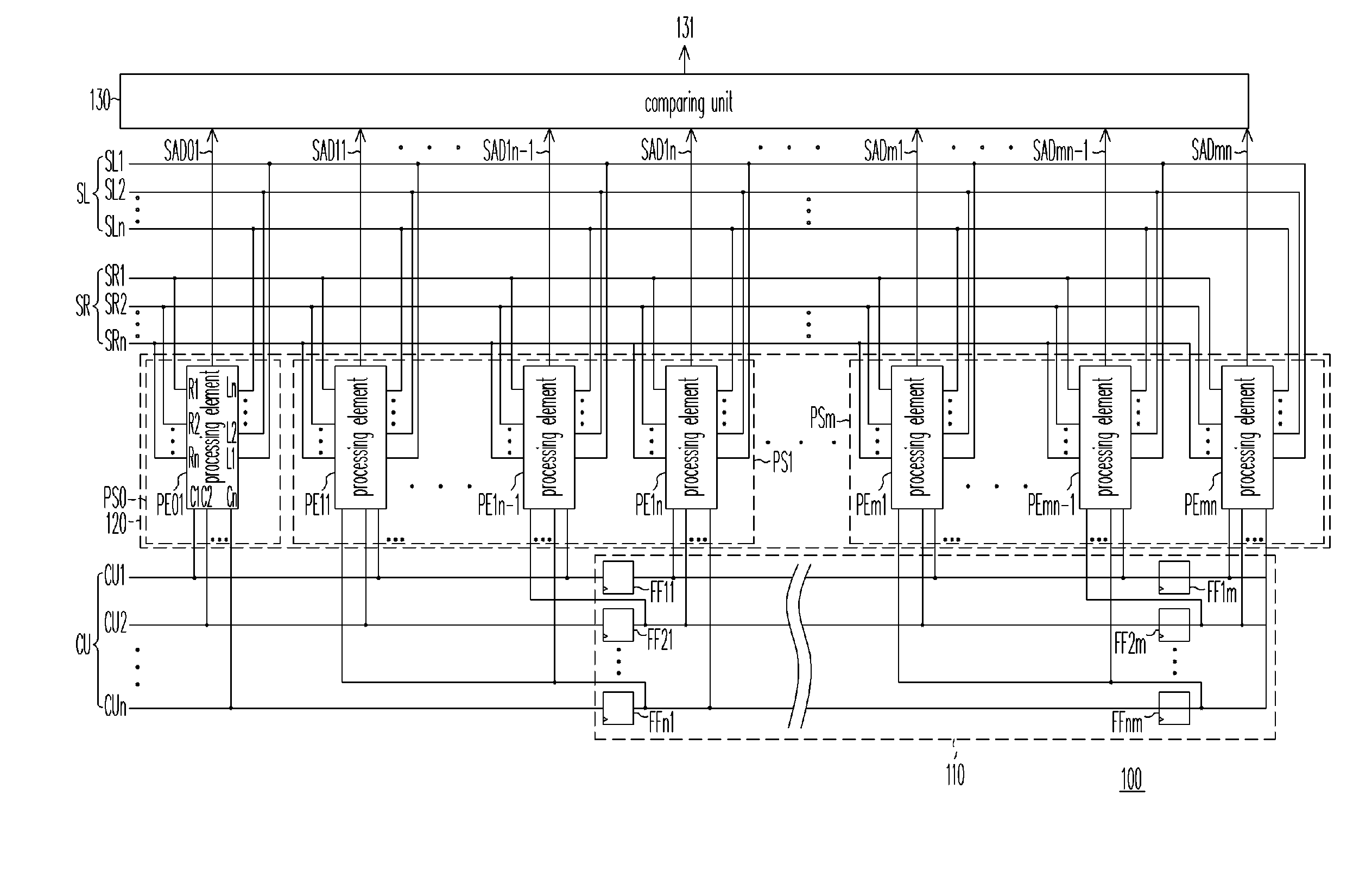
[0027]FIG. 1 is a schematic motion estimation circuit according to an embodiment. Referring to FIG. 1, a motion estimation circuit 100 is for searching a block in a search window (for example, the search window SW in FIG. 4) most similar to the current block (for example, the current block CU in FIG. 4). Wherein, the search window is formed by a left search window (for example, the left search window SL in FIG. 4) and a right search window (for example, the right search window SR in FIG. 4).

[0028] In the motion estimation circuit 100, a latch module 110 has n pieces of shift registers (n is an integer larger than 1) and each shift register has m stages of latches (m is an integer larger than 0). For example, the latches FF11˜FF1m, the latches FF21˜FF2m until the latches FFn1˜FFnm form n pieces of m-th stage shift registers. Each shift register receives and transmits a current block data CU to next stage according to a timing, wherein every latch is a, for example, D-type flip-flop....


PUM


Abstract

A motion estimation circuit and a motion estimation processing element are provided. The latch module in the motion estimation circuit has n pieces of m-stage shift registers. Each shift register receives a current block data and transmits the received current block data to next stage according to a timing. The processing module has a plurality of processing elements (PEs), which are divided into (m+l) groups. The PEs of the i-th group receive the left search window data and the right search window data and are coupled to the input ends and the output ends of the i-th stage of latches, wherein 0<i≦m. Each PE compares the similarity degree between the corresponding candidate block in the search window and the current block and outputs the processed result, respectively. The comparing unit receives and compares the processed results for outputting a first comparison result.

Description

CROSS-REFERENCE TO RELATED APPLICATION [0001] This application claims the priority benefit of Taiwan application serial no. 94140034, filed on Nov. 15, 2005. All disclosure of the Taiwan application is incorporated herein by reference. BACKGROUND OF THE INVENTION [0002] 1. Field of Invention [0003] The present invention relates to a motion estimation circuit, and particularly to a motion estimation circuit (ME circuit) and a motion estimation processing element (ME processing element), which combines both the advantage of a systolic array architecture featuring high efficiency of data reusing and the advantage of an adder-tree architecture featuring capability of simultaneously processing multi-point data in a clock cycle, so that high-efficient motion estimation operations are achieved. [0004] 2. Description of the Related Art [0005] Conventional motion estimation circuit (ME circuit) architectures can be mainly categorized into an adder-tree architecture and a systolic array archi...

Claims


Application Information

Patent Timeline
Patent Type & Authority Applications(United States)
IPC IPC(8): H04N11/04H04N7/12G06T1/20G06T7/20H04N19/136H04N19/137H04N19/196H04N19/436H04N19/50H04N19/51
CPCG06T7/2013H04N5/145G06T7/223
Inventor YANG, HSING-CHIEN
Owner NOVATEK MICROELECTRONICS CORP
Why Eureka
Try Eureka