Semiconductor memory device, information processing system including the same, and controller

a memory device and memory technology, applied in the direction of information storage, static storage, digital storage, etc., can solve the problems of reducing the utilization efficiency of a data bus, unable to read data from another bank, so as to reduce the increase of reduce the number of terminals, and maximize the use

Active Publication Date: 2012-09-25
LONGITUDE LICENSING LTD
View PDF5 Cites 8 Cited by
  • Summary
  • Abstract
  • Description
  • Claims
  • Application Information

AI Technical Summary

Benefits of technology

[0015]As explained above, in the semiconductor memory device according to the present invention, a plurality of memory circuit units are provided and a data input / output terminal is allocated to each memory circuit unit. Therefore, read data can be output from a certain memory circuit unit while read data is being output from another memory circuit unit. This is also the same in a write operation. With this configuration, because unnecessary read data or unnecessary write data does not have to be transferred, utilization efficiency of a data bus can be increased. Furthermore, because an address terminal is common to a plurality of memory circuit units, increase of the number of terminals can be minimized.
[0016]Further, because the controller can handle one semiconductor memory device as plural chips, a data bus can be efficiently used without making an information processing system complex.

Problems solved by technology

However, because these bank share a data input / output terminal, read data cannot be output from another bank during a period when read data is being output from a certain bank.
Therefore, even when a part of bits of read data output from a certain bank is unnecessary for the controller, read data cannot be output from another bank until when a series of burst output are finished.
Frequent occurrence of such situations lowers utilization efficiency of a data bus, resulting in a problem that an effective data transfer rate is decreased.
Meshed data is necessary data, and unmeshed data is unnecessary data.
While a problem in the read operation has been explained with reference to FIG. 9, this problem also occurs in a write operation.
This kind of problem occurs noticeably in multibit products having a large number of I / O bits.

Method used


Image

  • Semiconductor memory device, information processing system including the same, and controller
  • Semiconductor memory device, information processing system including the same, and controller
  • Semiconductor memory device, information processing system including the same, and controller

Examples


first embodiment

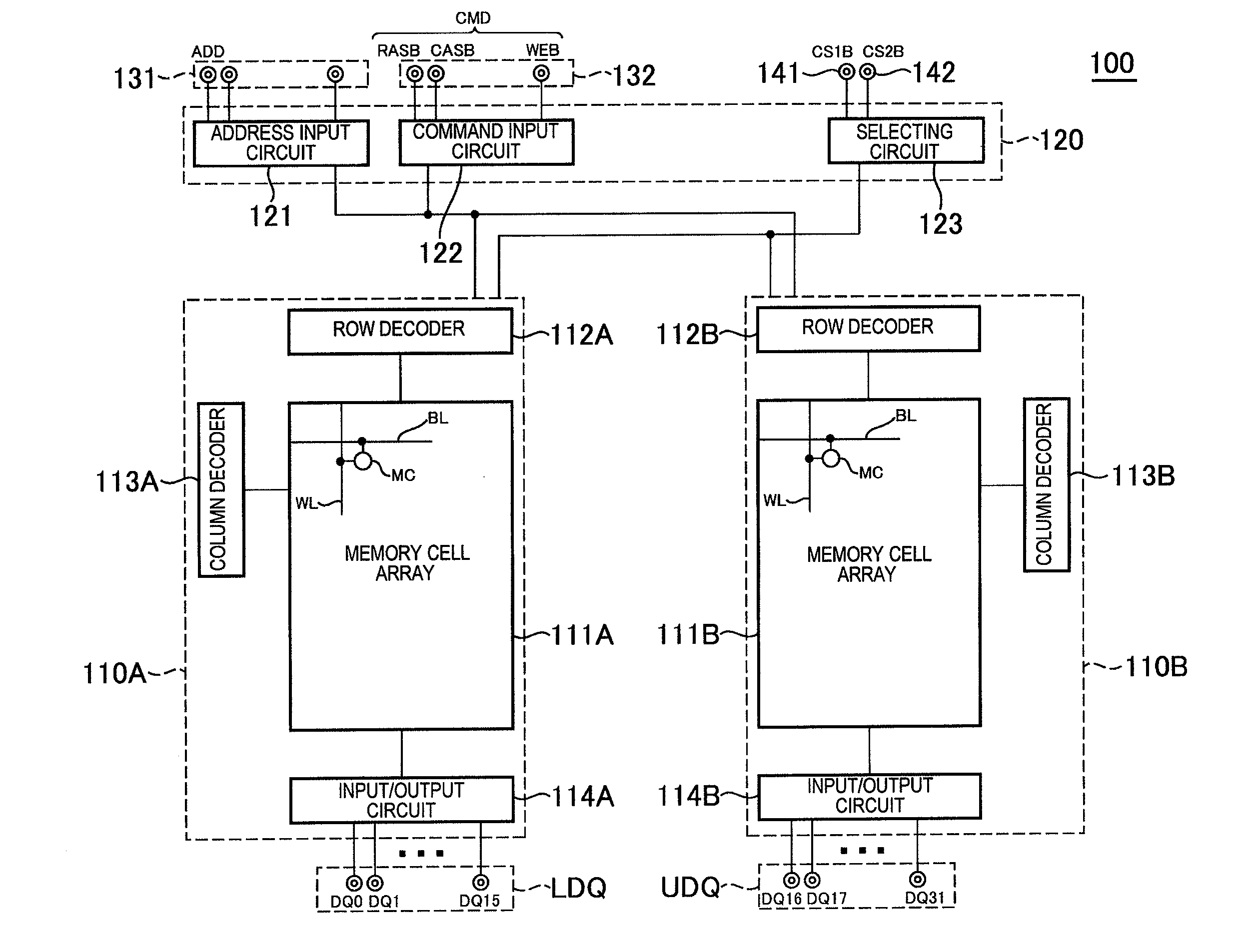
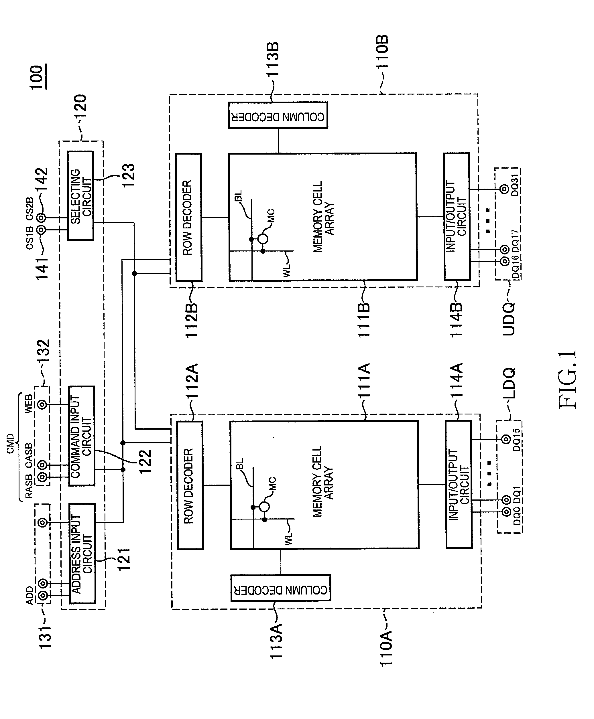
[0031]As shown in FIG. 1, the semiconductor memory device 100 includes two memory circuit units 110A and 110B, and a common circuit 120 allocated in common to these memory circuit units 110A and 110B. The memory circuit units 110A and 110B are circuit blocks capable of mutually independently performing a read operation and a write operation. A data input / output terminal group LDQ is allocated to the memory circuit unit 110A, and a data input / output terminal group UDQ is allocated to the memory circuit unit 110B. The data input / output terminal group LDQ includes 16 data input / output terminals DQ0 to DQ15. The data input / output terminal group UDQ includes 16 data input / output terminals DQ16 to DQ31.

[0032]In this way, the semiconductor memory device 100 according to the first embodiment is a single memory (a memory integrated on a single semiconductor substrate) having 32 bits (DQ0 to DQ31) for I / O. A half of the data input / output terminals (DQ0 to DQ15) are allocated to the memory ci...

second embodiment

[0083]the present invention is explained next.

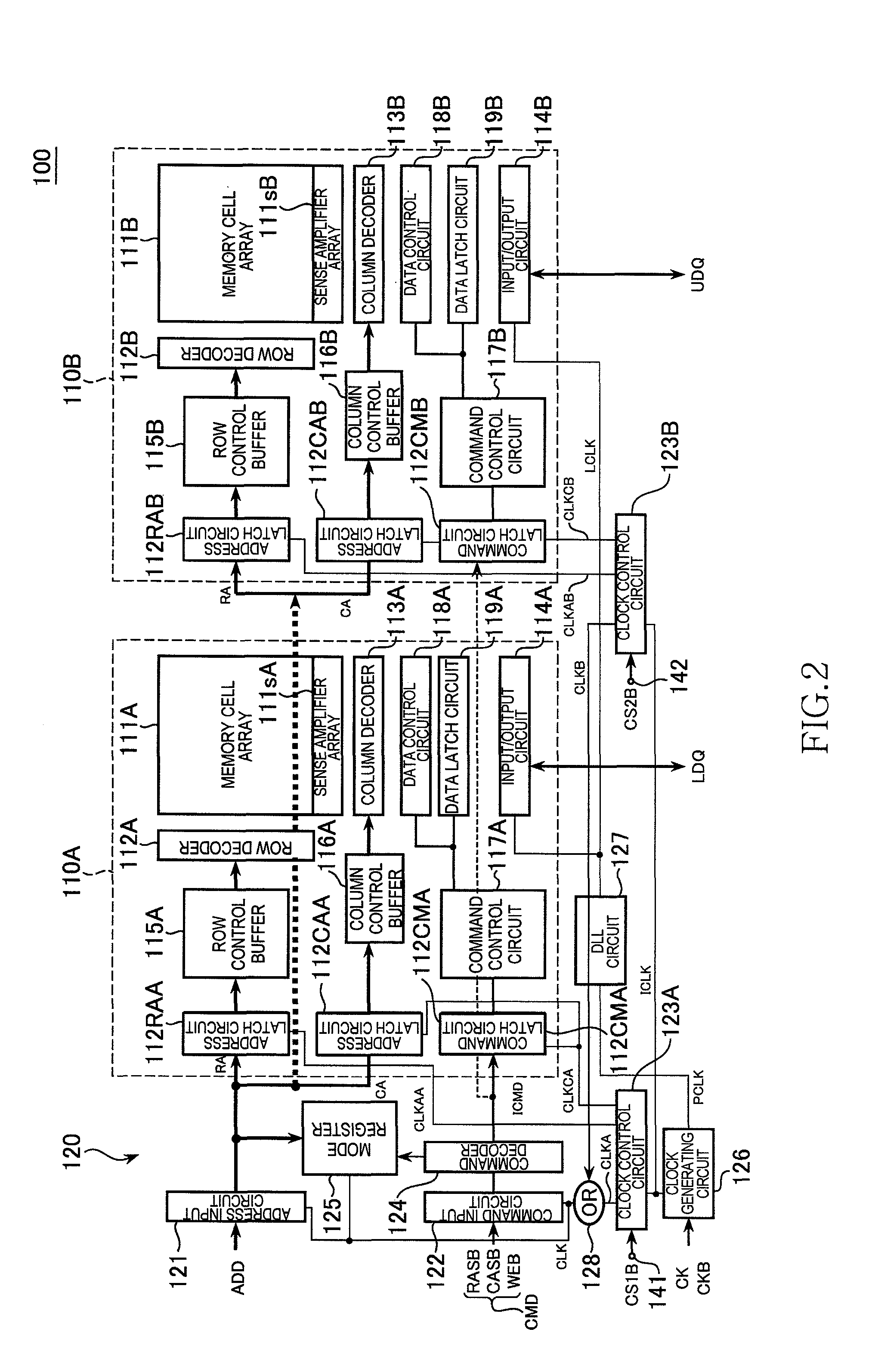
[0084]FIG. 7 is a block diagram showing a configuration of a semiconductor memory device 300 according to the second embodiment.

[0085]The semiconductor memory device 300 according to the second embodiment is different from the semiconductor memory device 100 in that two mode registers 125 are provided. Other features of the semiconductor memory device 300 are identical to those of the semiconductor memory device 100 described above, therefore like reference characters are denoted to like elements and redundant explanations thereof will be omitted.

[0086]Mode registers 125A and 125B included in the semiconductor memory device 300 according to the second embodiment are circuits to set operation modes of the memory circuit units 110A and 110B, respectively. That is, in the second embodiment, an operation mode of the memory circuit unit 110A and an operation mode of the memory circuit unit 110B can be set separately.

[0087]FIG. 8 is a timing d...


PUM


Abstract

To include first and second data input / output terminals allocated to first and second memory circuit units, respectively, and an address terminal allocated in common to these memory circuit units. When a first chip selection signal is activated, the first memory circuit unit performs a read operation or a write operation via the first data input / output terminal based on an address signal regardless of an operation of the second memory circuit unit. When a second chip selection signal is activated, the second memory circuit unit performs a read operation or a write operation via the second data input / output terminal based on the address signal regardless of an operation of the first memory circuit unit. With this configuration, a wasteful data transfer can be prevented, and the effective data transfer rate can be increased.

Description

BACKGROUND OF THE INVENTION[0001]1. Field of the Invention[0002]The present invention relates to a semiconductor memory device and an information processing system including the same, and more particularly relates to a semiconductor memory device having a plurality of memory circuit units operable independently of each other and an information processing system including the semiconductor memory device. The present invention also relates to a controller that controls the semiconductor memory device.[0003]2. Description of Related Art[0004]Many DRAMs (Dynamic Random Access Memories) as representative semiconductor memory devices have their internal portions divided into plural banks in order to enable parallel operations (see Japanese Patent Application Laid-open No. H11-66841). A controller connected to the DRAMs can individually issue a command to each bank, and when a certain bank is performing a read operation or a write operation, the controller can issue commands to another ban...

Claims


Application Information

Patent Timeline
Patent Type & Authority Patents(United States)
IPC IPC(8): G11C7/00
CPCG11C7/10G11C7/22G11C11/4096G11C11/4093G11C11/4076
Inventor TAKAHASHI, YASUSHIISHIKAWA, TORU
Owner LONGITUDE LICENSING LTD
Why Eureka
Try Eureka