Circuit design system and circuit design program

a circuit design and circuit technology, applied in the field of circuit design system and circuit design system program, can solve the problems of low occurrence rate and unnecessarily inserting observation points, and achieve the effect of fewer observation points, efficient facilitation of failure analysis, and improved failure analysis

Active Publication Date: 2007-05-17
RENESAS ELECTRONICS CORP
View PDF4 Cites 15 Cited by
  • Summary
  • Abstract
  • Description
  • Claims
  • Application Information

AI Technical Summary

Benefits of technology

[0015] According to the present invention, the judgment module decides the target node based on the number Ji. For example, it is highly possible that a probability of fault occurrence in an equivalent fault class Gi having the maximum node number Ji takes a maximum value among all the equivalent fault classes G1 to GI. Therefore, the judgment module can select the target node from the equivalent fault class Gi having the maximum node number Ji. By inserting the observation point preferentially into the equivalent fault class including a lot of equivalent fault nodes, it is possible to “efficiently” reduce the number of fault candidates as a whole. In other words, it is possible to improve the failure-analyticity with fewer observation points.
[0017] According to the present invention, as described above, the observation point is preferentially inserted into an equivalent fault class Gi that has relatively large parameter Di. As a result, the failure-analyticity can be improved “efficiently”. That is, the failure-analyticity is improved even with the small number of observation points. In other words, it is possible to optimize the observation-point insertion positions and to facilitate the failure analysis with the small number of observation points.
[0020] According to the circuit design system and the circuit design program of the present invention, the insertion position into which the observation point is inserted is optimized. As a result, the failure-analyticity is improved even with the small number of observation points inserted. In other words, it is possible to efficiently facilitate the failure analysis with fewer observation points.
[0021] Furthermore, the circuit design system and the circuit design program according to the present invention can be applied to the physical synthesis design method. That is, even in a case where the physical synthesis method is employed, it is possible to facilitate the failure analysis by inserting the observation point.

Problems solved by technology

Therefore, there is a possibility that the observation point is unnecessarily inserted into a node at which the fault occurrence rate is low.

Method used


Image

  • Circuit design system and circuit design program
  • Circuit design system and circuit design program
  • Circuit design system and circuit design program

Examples


first embodiment

1. First Embodiment

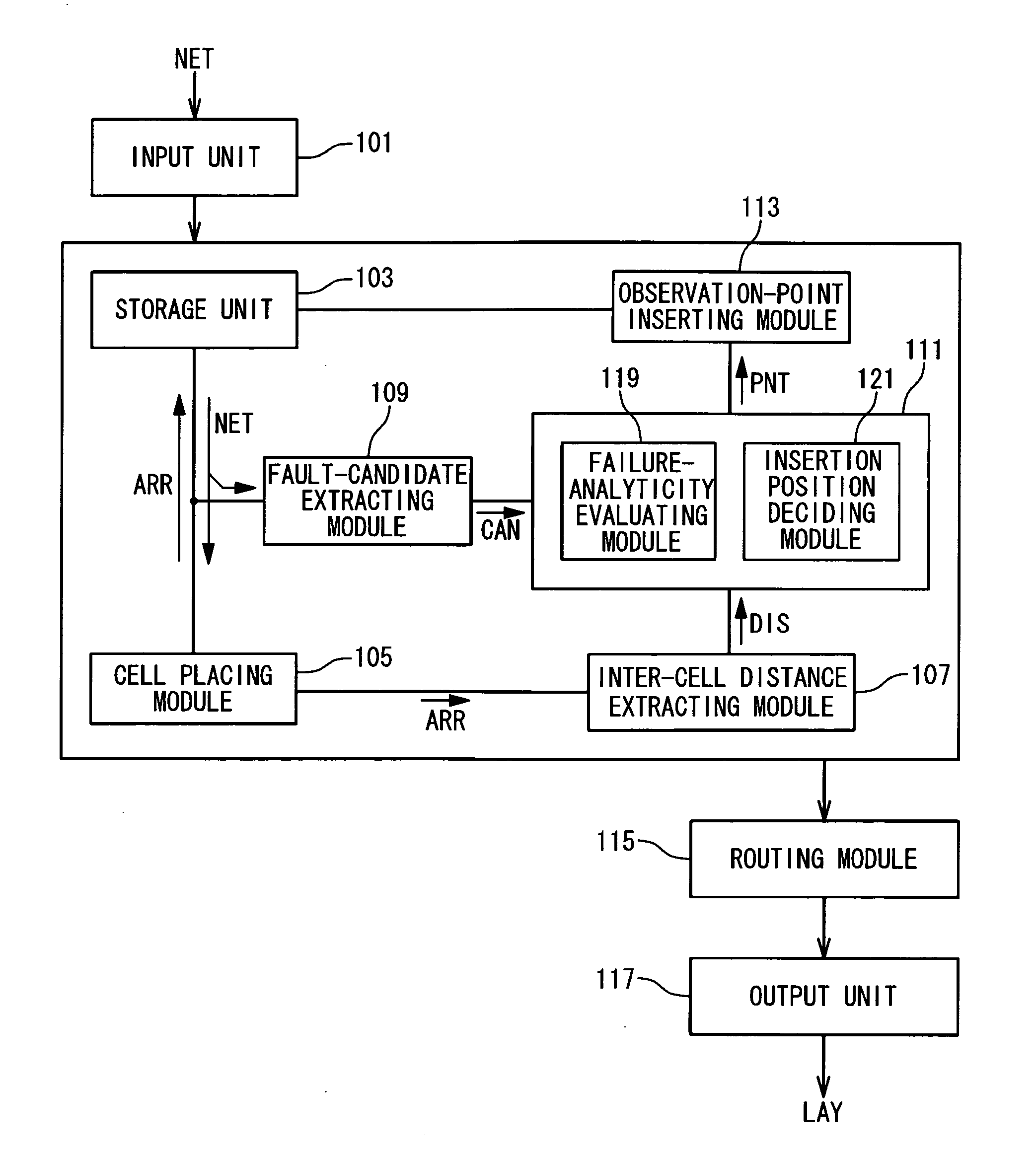
[0052]FIG. 3 is a block diagram showing a configuration of a circuit design system (a failure analysis facilitating design system) according to a first embodiment of the present invention. The circuit design system shown in FIG. 3 generates a layout data LAY indicating a layout of a design-target circuit from a netlist NET indicating connection information of the design-target circuit. The circuit design system can be realized by, for example, a processing unit, a storage unit, and a computer program (circuit design program) executed by the processing unit.

[0053] Firstly, a general description will be given on the circuit design system according to the present embodiment. As shown in FIG. 3, the circuit design system has an input unit 101, a storage unit 103, a cell placing module 105, an inter-cell distance extracting module 107, a fault-candidate extracting module 109, a judgment module 111, an observation-point inserting module 113, a routing module 115, and a...

second embodiment

2. Second Embodiment

[0112]FIG. 14 is a block diagram showing a configuration of a circuit design system (a failure analysis facilitating design system) according to a second embodiment of the present invention. The circuit design system according to the present embodiment has the input unit 101, the storage unit 103, the cell placing module 105, the fault-candidate extracting module 109, the judgment module 111, the observation-point inserting module 113, the routing module 115, and the output unit 117. In FIG. 14, the same reference numerals are given to the same components as those described in the first embodiment, and an overlapping description will be appropriately omitted.

[0113] The second embodiment differs from the first embodiment in that the circuit design system does not include the inter-cell distance extracting module 107. Furthermore, in the second embodiment, the cell placing module 105 places cells after all the necessary observation points are inserted.

[0114]FIG. ...

third embodiment

3. Third Embodiment

[0122]FIG. 16 is a block diagram showing a configuration of a circuit design system (a failure analysis facilitating design system) according to a third embodiment of the present invention. The circuit design system according to the present embodiment has the input unit 101, the storage unit 103, the fault-candidate extracting module 109, a layout module 135, a judgment module 111, the observation-point inserting module 113, and the output unit 117. The layout module 135 includes the cell placing module 105 and the routing module 115. The judgment module 111 includes not only the failure-analyticity evaluating module 119 and the insertion position deciding module 121 but also a structure extracting module 123. In FIG. 16, the same reference numerals are given to the same components as those described in the first embodiment, and an overlapping description will be appropriately omitted.

[0123] The third embodiment differs from the first embodiment in that the circu...


PUM


Abstract

A circuit design system has: a storage unit in which a netlist is stored; a fault-candidate extracting module configured to extract equivalent fault class Gi from the netlist; a judgment module configured to select a target node out of a plurality of nodes Ni1 to Niji included in the equivalent fault class Gi, wherein Ji is a number of nodes included in the equivalent fault class Gi; and an observation-point inserting module configured to update the netlist by inserting at least one observation point into the target node. The judgment module decides the target node based on the number Ji.

Description

BACKGROUND OF THE INVENTION [0001] 1. Field of the Invention [0002] The present invention relates to a circuit design system and a circuit design system program used in designing a logic circuit. In particular, the present invention relates to a circuit design system and a circuit design system program used for facilitating a failure analysis. [0003] 2. Description of the Related Art [0004] In an ordinary process of manufacturing semiconductor integrated circuits, defective products are included in the manufactured semiconductor integrated circuits to some degree. The defective products are eliminated in a test process and only non-defective products are shipped. Here, a rate of the non-defective products at this time is referred to as “yield”. If the yield is low, then cost of manufacturing goods is increased and profit is declined. It is therefore necessary to establish a cause of the defect by a failure analysis and to enhance the yield by improving the manufacturing process. [00...

Claims


Application Information

Patent Timeline
Patent Type & Authority Applications(United States)
IPC IPC(8): G01R31/28
CPCG06F17/505G06F30/327
Inventor NONAKA, JUNPEI
Owner RENESAS ELECTRONICS CORP
Why Eureka
Try Eureka