Monolithic bypass diode and photovoltaic cell with bypass diode formed in back of substrate

a monolithic bypass diode and photovoltaic cell technology, applied in the direction of diodes, semiconductor devices, electrical devices, etc., can solve the problems of increasing the weight and complexity of the solar cell structure, reducing the efficiency new failure points of the solar cell, so as to minimize the need for additional wiring and/or metallization, the effect of maximizing the solar cell area

Active Publication Date: 2007-05-24
THE BOEING CO
View PDF10 Cites 64 Cited by
  • Summary
  • Abstract
  • Description
  • Claims
  • Application Information

AI Technical Summary

Benefits of technology

[0015] The present invention provides a solar cell that has an integrated bypass diode. The present invention also provides a solar cell that has a bypass diode that minimize

Problems solved by technology

Solar cells are typically long-life devices, but can have their efficiency reduced or destroyed by reverse biasing of the solar cell junction.
The use of additional wiring and/or additional metallization creates new failure points for solar cells, as well as adding to the weight and complexity of the solar cell structure.
Additional weight and failure mechanisms are unacceptable in a spacecraft environment, because of the extreme additional costs involved.
Further, additional metallization obscures the solar cell from receiving in

Method used


Image

  • Monolithic bypass diode and photovoltaic cell with bypass diode formed in back of substrate
  • Monolithic bypass diode and photovoltaic cell with bypass diode formed in back of substrate
  • Monolithic bypass diode and photovoltaic cell with bypass diode formed in back of substrate

Examples


Embodiment Construction

[0025] In the following description, reference is made to the accompanying drawings which form a part hereof, and which is shown, by way of illustration, several embodiments of the present invention. It is understood that other embodiments may be utilized and structural changes may be made without departing from the scope of the present invention.

Overview

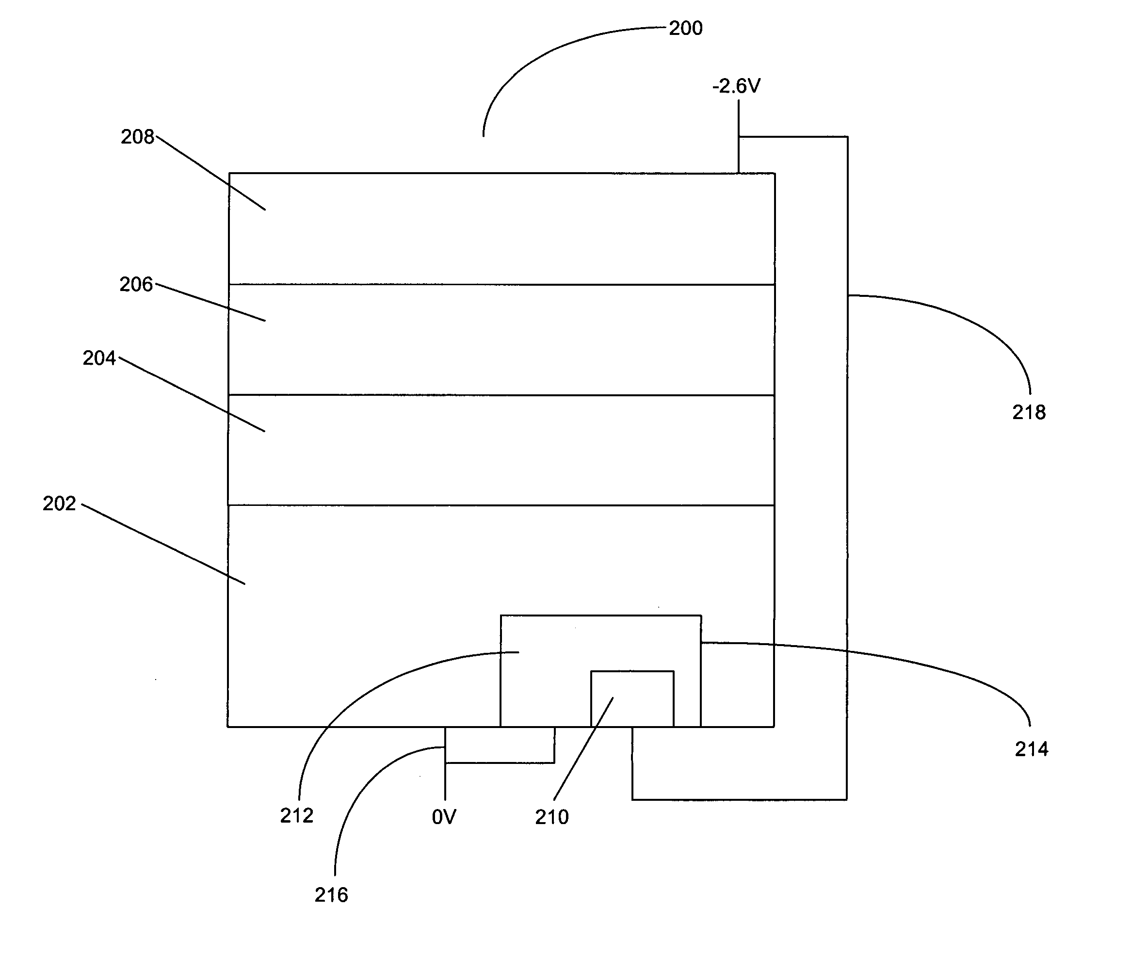
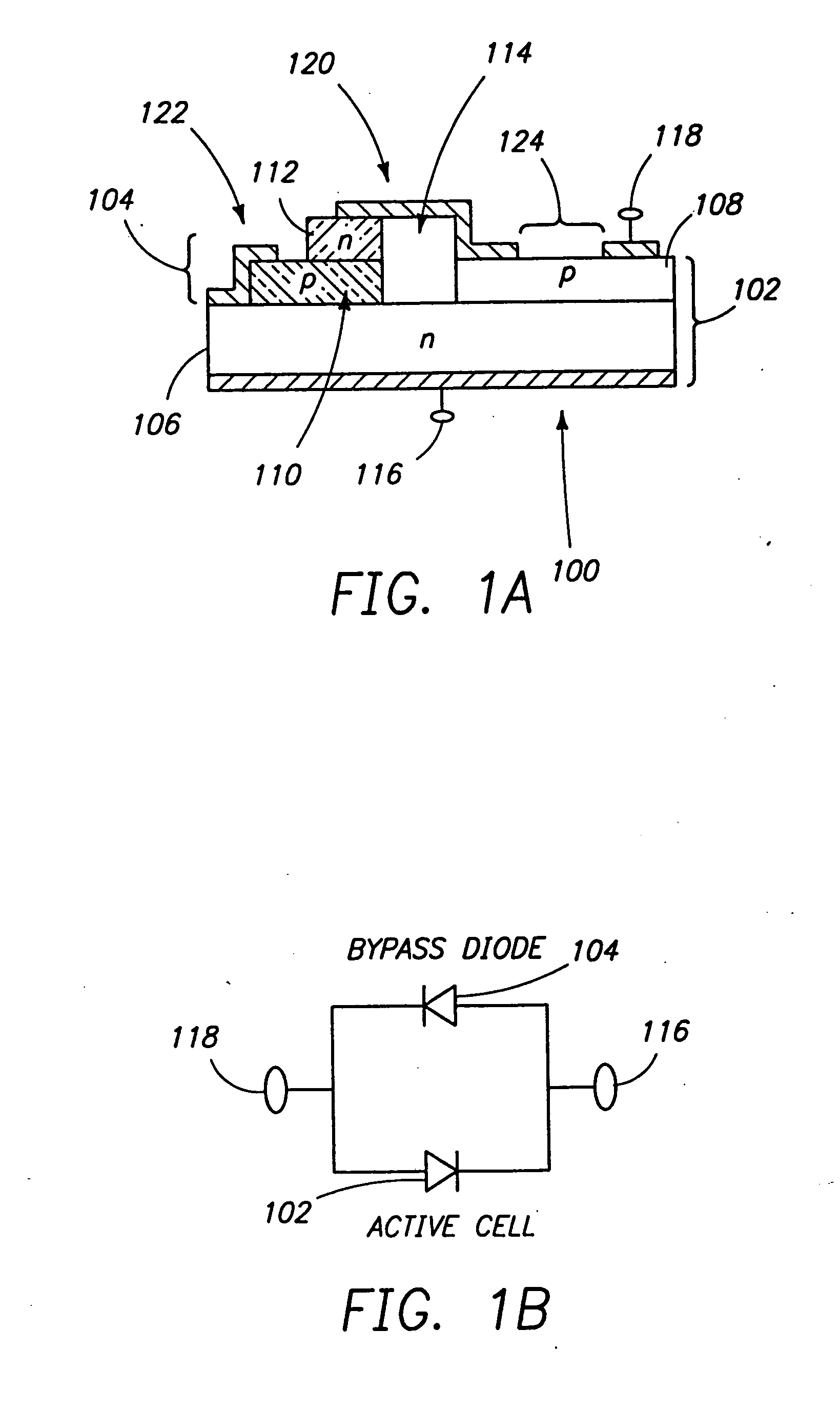
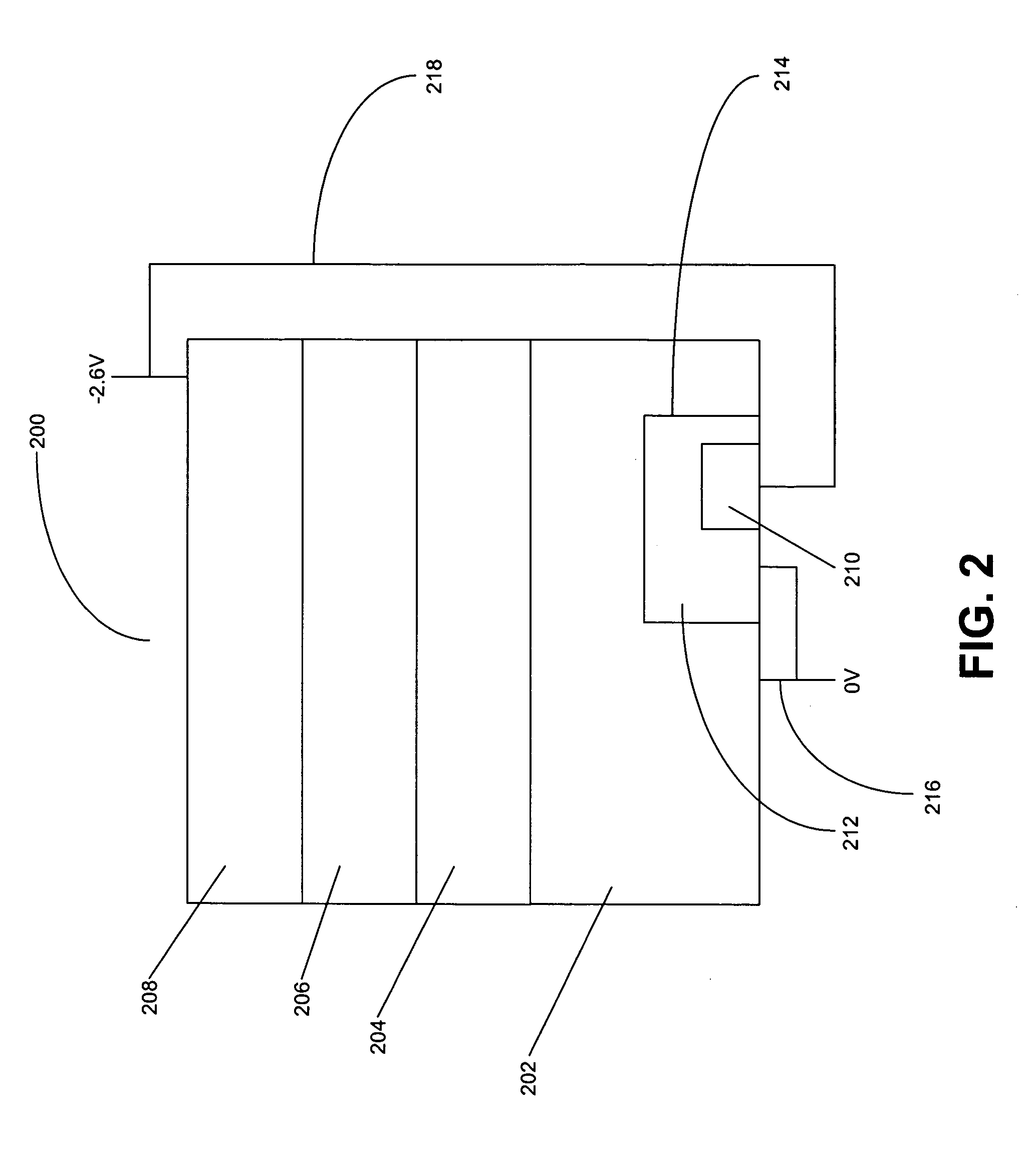
[0026] The present invention monolithically incorporates a bypass diode into a solar cell assembly. The present invention creates the bypass diode without complex processing steps, which increases the yield for the finished device.

[0027] Prior art processes, such as those described in U.S. Pat. No. 5,616,185, entitled “SOLAR CELL WITH INTEGRATED BYPASS DIODE AND METHOD,” describe using a discrete bypass diode that is integrated with the solar cell as a hybrid assembly. The bypass diode is integrated with the solar cell by forming recesses on the non-illuminated side of the solar cell and placing at least one discrete low-profile...


PUM


Abstract

An apparatus and method for making a solar cell assembly. An apparatus in accordance with the present invention comprises a substrate, at least a first solar cell, coupled to a first side of the substrate, the first side of the substrate to be exposed to light such that the at least first solar cell generates a current when exposed to the light, and a bypass diode, formed on a second side of the substrate, the second side of the substrate being substantially opposite the first side of the substrate, such that the bypass diode is monolithically integrated with the at least first solar cell.

Description

BACKGROUND OF THE INVENTION [0001] 1. Field of the Invention [0002] The present invention relates to devices and methods for making semiconductor devices, and in particular to a device and method for making monolithic bypass-diodes and solar cell string assemblies. [0003] 2. Description of the Related Art [0004] Solar cells are used in various technologies to provide power to other electronic assemblies. Satellites, calculators, and power systems are all examples of solar cell usage. [0005] A solar cell is a p-n junction created over a large area on a semiconductor substrate. The junction creates a voltage and current when light of certain wavelengths strike the surface of the solar cell, and, as such, solar cells are photovoltaic devices. These photovoltaic cells provide a lightweight, maintenance-free power source for various applications, and also provide a pollution-free, distributed energy generation source for use in power delivery systems. [0006] Solar cells are typically lon...

Claims


Application Information

Patent Timeline
IPC IPC(8): H01L31/00
CPCH01L27/142H01L31/0725Y02E10/50H01L31/0445
Inventor KINSEY, GEOFFREY S.KING, RICHARD R.KRUT, DMITRI D.KARAM, NASSAR H.
Owner THE BOEING CO
Why Eureka
Try Eureka