Light emitting device

a light-emitting device and light-emitting technology, which is applied in the manufacture of semiconductor/solid-state devices, semiconductor devices, electrical devices, etc., can solve the problems of large chip mounts, difficult to mount chips with large size, and large light-emitting mounts, etc., and achieve high light-emitting efficiency and thin body

Inactive Publication Date: 2007-05-24
LEDCOMM LLC
View PDF18 Cites 39 Cited by
  • Summary
  • Abstract
  • Description
  • Claims
  • Application Information

AI Technical Summary

Benefits of technology

[0022] In view of the foregoing problems, the present invention has an object of providing a light emitting device, which has a thin body and achieves high light extraction efficiency.
[0023] Further, in view of the foregoing problems, the present invention has an object of providing a light emitting device, which has a thin body including a large wire bonding region and a large die bonding region, and which achieves high light extraction efficiency.

Problems solved by technology

Thus, in the light emitting devices described in these publications, light extraction efficiency has not been sufficient when such a chip is used.
This narrows the area for the wire bonding region, causing difficulties in performing wire bonding.
Further, since the die bonding region is narrow, it has been difficult to mount a chip being large in size and emitting large mount of light.
Further, the light emitting device described in Patent Document 2 does not consider to provide a thin light emitting devices by forming the reflector in a compressed shape.

Method used


Image

  • Light emitting device
  • Light emitting device
  • Light emitting device

Examples


first embodiment

[0049] Referring to FIGS. 1 through 4, the following describes an embodiment of a light emitting device according to the present invention.

[0050]FIG. 1(a) is a cross-sectional view of the light emitting device according to the present embodiment.

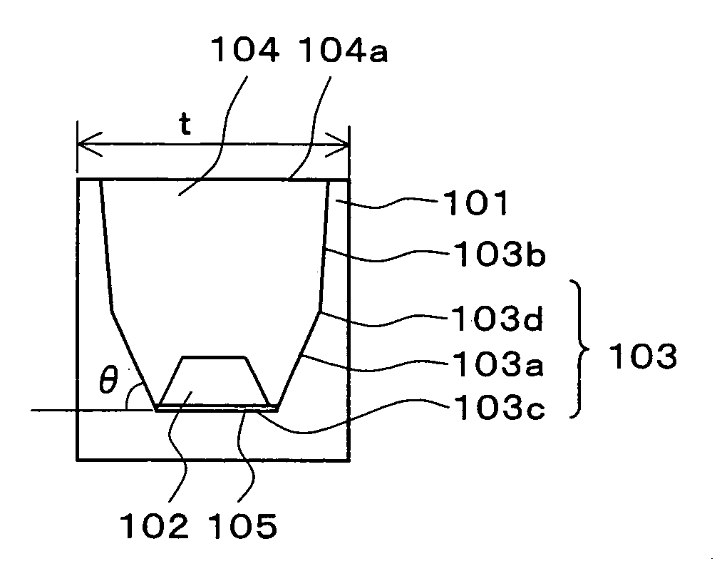
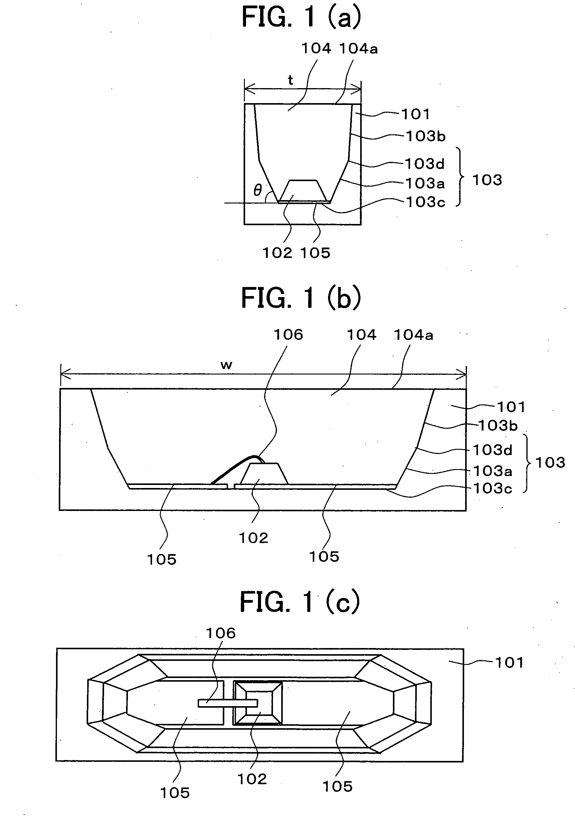
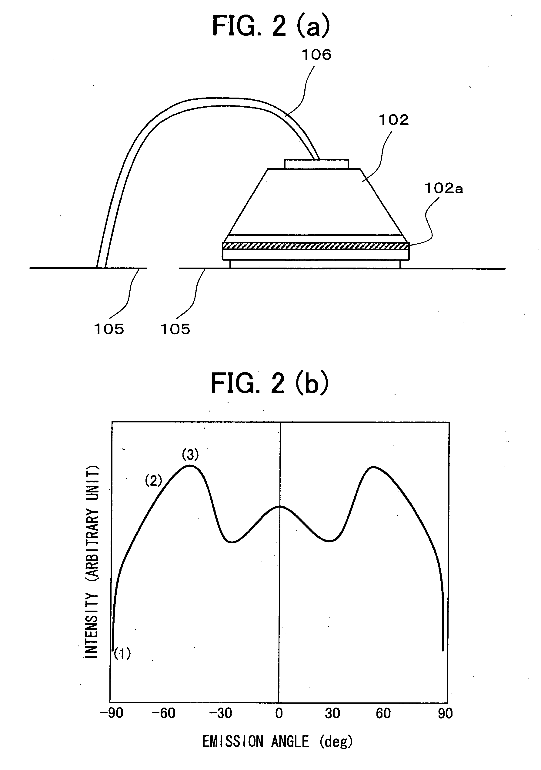
[0051] The light emitting device includes: a substantially rectangular package body (hereinafter referred to as package 101) having a dish-shaped concave portion; and an LED chip (hereinafter referred to as chip 102) shown in FIG. 2(a).

[0052] The concave portion constitutes a reflector 103 having a bottom surface 103c and a side wall provided with an angle along an outer edge of the bottom surface. In order to have a reflector function, the reflector 103 may utilize reflection characteristics of the package 101 itself in a case where the package 101 is constituted by a white package, or may separately process a side wall of the concave portion so as to improve reflectivity of the concave portion. For example, a reflective film may be form...

second embodiment

[0092] Referring to FIGS. 5 through 9, the following describes another embodiment of a light emitting device according to the present invention.

[0093]FIG. 5(a) is a cross sectional view of the light emitting device according to the present embodiment.

[0094] The light emitting device includes: a rectangular package body having a dish-shaped concave portion (hereinafter referred to as package 201); and a chip 202 having a light emitting section, i.e., an active layer, formed in the vicinity of a top surface of the chip 202 as shown in FIG. 5(a) (hereinafter referred to as junction up chip).

[0095] The concave portion constitutes a reflector 203 having a depressed region and an inclined plane provided along an edge of the depressed region.

[0096] The depressed region has a bottom surface 203e and a vertical plane 203a provided along an outer edge of the 203e so as to be substantially vertical to the bottom surface 203e.

[0097] The depressed region has a depth being substantially equi...


PUM


Abstract

A light emitting device includes: a light emitting element; and a substantially rectangular package body in which the light emitting element is contained and a concave portion is formed. The concave portion has a bottom surface on which the light emitting element is disposed, and is filled with a transparent sealing resin for covering the light emitting element. Further, the sealing resin has a surface serving as an emitting surface, from which light is extracted. The package body includes: a reflection surface being an inclined plane provided along a short side of a depressed region toward the emitting surface, when seen from above the emitting surface; and a die bonding region and a wire bonding region on a bottom surface of the depressed region. Further, the depressed region has a depth being substantially equal to or less than a height of the active layer of the light emitting element.

Description

[0001] This Nonprovisional application claims priority under 35 U.S.C. § 119(a) on Patent Applications No. 336402 / 2005 and 336403 / 2005 both filed in Japan on Nov. 21, 2005, the entire contents of which are hereby incorporated by reference. FIELD OF THE INVENTION [0002] The present invention relates to a light emitting device including a light emitting element and a package body which contains the light emitting element and in which a concave portion having a reflector function for extracting light to the outside is formed. BACKGROUND OF THE INVENTION [0003] As a thin plane light source used in liquid crystal displays, for example, there has been a surface mount light emitting device (hereinafter referred to as light emitting device), which is disposed on an edge surface of an optical waveguide provided on a bottom surface of a liquid crystal display unit. [0004] In the plane light source, the optical waveguide and the light emitting device are provided so that the edge surface of th...

Claims


Application Information

Patent Timeline
Patent Type & Authority Applications(United States)
IPC IPC(8): H01L29/06
CPCH01L33/60H01L2224/48091H01L2224/49107H01L2924/00014
Inventor ITO, SHIN
Owner LEDCOMM LLC
Why Eureka
Try Eureka