Waveguide tube formed by laminating a plate and substrates having waveguide passages

a technology of waveguide tube and substrate, applied in the direction of waveguides, multiple-port networks, electrical devices, etc., can solve the problems of increased thickness of the device, and difficulty in manufacturing the device. , to achieve the effect of thin body

Active Publication Date: 2012-03-13
DENSO CORP
View PDF11 Cites 6 Cited by
  • Summary
  • Abstract
  • Description
  • Claims
  • Application Information

AI Technical Summary

Benefits of technology

[0009]The present invention has been developed to solve the above described issues. An object of the present invention is to provide a high frequency signal transmitting device having a lightweight and thin body. To achieve the above-described object, a high frequency device equipped with a waveguide tube unit that transmits a high frequency signal, the waveguide having a rectangular waveguide passage through which the high frequency signal is transmitted, the waveguide passage extending in a longitudinal direction thereof and having a rectangle section cut perpendicularly to the longitudinal direction, the rectangle section consisting of short side edges and long side edges, the device comprising: a plate having a thickness corresponding to a length of the short side edges of the waveguide passage and having a through hole formed through the mutually-opposite surfaces of the plate in a direction of the thickness, the through hole having a width perpendicular to the longitudinal direction, having an inner wall and openings opened at the surfaces, wherein at least the inner wall and edges of the openings are given electrical conductivity; and a pair of substrates, each substrate being made of resin and laminated on each of the mutually-opposite surfaces of the plate and having grounding patterns connected to the ground, the grounding pattern being located at a specified region of a surface of each of the substrates, the specified region positionally corresponding to the waveguide passage formed in the plate, the plate and the pair of substrates composing the waveguide tube unit.

Problems solved by technology

In this regard, it is required to process the metallic plate to be a complex shape, which makes manufacturing the device difficult.
In addition, the high frequency device having joined metallic plates has problems such as being heavy, and requiring an additional high frequency circuit board for processing signals being transmitted through the waveguide tube.
Furthermore, there can be a problem that thickness of the device is increased when the high frequency board is laminated to the metallic plates.

Method used


Image

  • Waveguide tube formed by laminating a plate and substrates having waveguide passages
  • Waveguide tube formed by laminating a plate and substrates having waveguide passages
  • Waveguide tube formed by laminating a plate and substrates having waveguide passages

Examples


first embodiment

[0029](First Embodiment)

[0030]Referring to FIGS. 1A, 1B 2A and 2B a first embodiment will now be described.

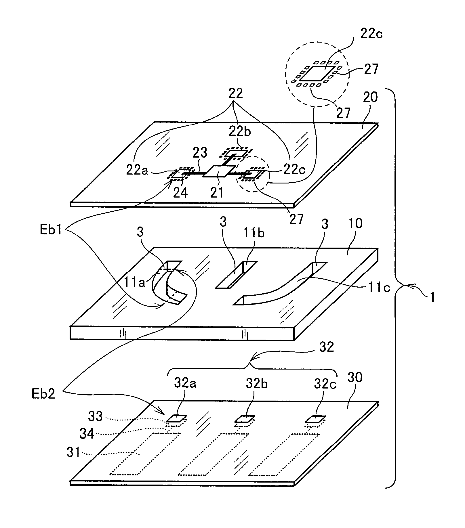
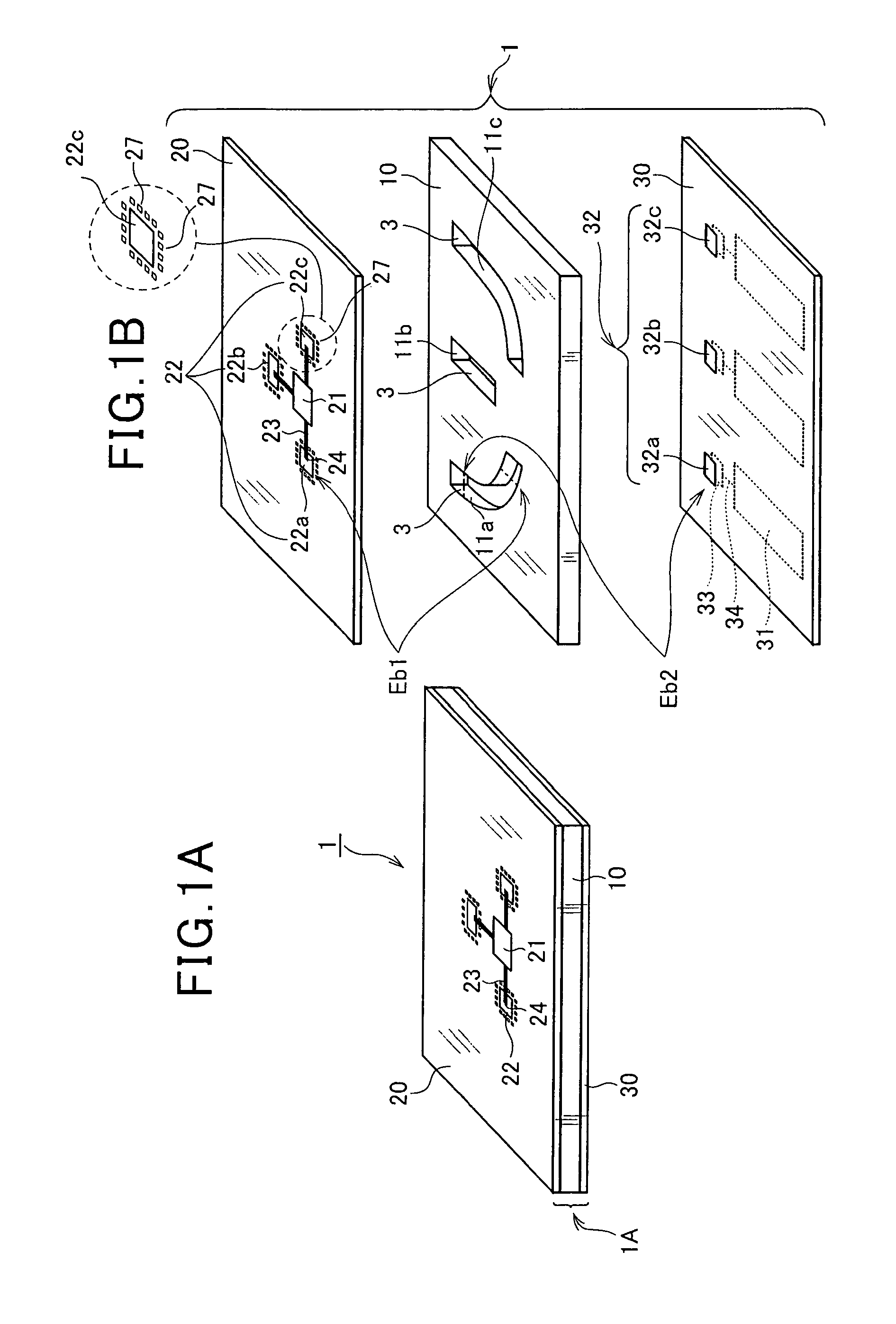
[0031]FIG. 1A is a perspective view showing an overall configuration of a high frequency signal transmitting device 1 to which the present invention is applied. FIG. 1B is an exploded perspective view showing the high frequency signal transmitting device 1.

[0032]The high frequency signal transmitting device 1, which serves as the high-frequency device according to the present invention, is applied to a radar device using millimeter waves and microwaves.

[0033]As shown in FIGS. 1A and 1B, the high frequency signal transmitting device 1 includes a waveguide plate 10, a first substrate 20, and a second substrate 30. A plurality (three according to the first embodiment) of through holes 11a, 11b and 11c as shown in FIG. 1B are formed on the waveguide plate 10 so as to form a rectangular waveguide passage 3. The waveguide plate is made of metallic plate (e.g. conductor). The first su...

second embodiment

[0045](Second Embodiment)

[0046]Next, referring to FIGS. 3A and 3B, a second embodiment will now be described.

[0047]In this embodiment, only a configuration of the waveguide plate 10 differs from that of the waveguide plate 10 according to the first embodiment. Therefore, a portion of the configuration that differs will mainly be described.

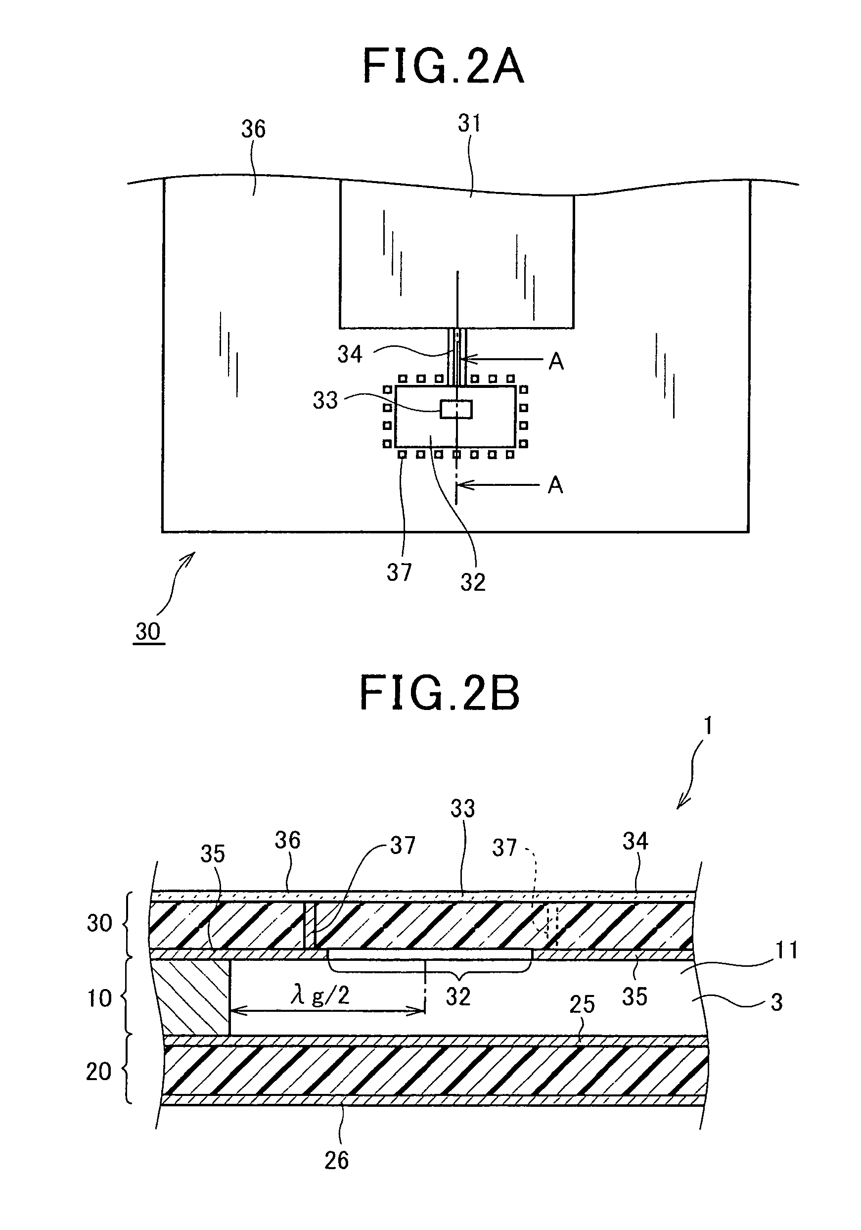
[0048]FIG. 3A is a planar view showing a joint surface of the waveguide plate 10 at which the waveguide plate 10 and the first substrate 20 are joined.

[0049]As shown in FIG. 3A, on the joint surface of the waveguide plate 10 at which the waveguide plate 10 and the first substrate 20 are joined, grooves 12a, 12b and 12c are arranged corresponding to respective through holes 11(11a to 11c). The grooves work as air passages that allow the air to flow between the rectangular waveguide passage 3 and outside space of the waveguide plate 10.

[0050]This groove 12a, 12b and 12c are formed such that end portions at a side of the through holes 11a, 11b and 11c...

third embodiment

[0057](Third Embodiment)

[0058]Next, referring to Figs. 4A, 4B and 4C, a third embodiment will now be described.

[0059]A high frequency signal transmitting device 5 of the third embodiment is configured as a slot array antenna.

[0060]FIG. 4A is a planar view showing a configuration of the high frequency signal transmitting device 5. FIG. 4B is a cross-sectional view showing a section along the B-B line taken in FIG. 4A. FIG. 4C is a planar view showing a joint surface of the first substrate at which the waveguide plate and the first substrate are joined.

[0061]As shown in FIG. 4B, the high frequency signal transmitting device 5 comprises a waveguide plate 40 which is made of metallic plate, having a through hole 41 used for a rectangular waveguide passage 7, and the first and second substrates 50, 60 as shown in FIG. 4C and 4A, respectively which are joined to opposite side of the waveguide plate 40.

[0062]Referring to FIG. 4B, the first substrate 50 is made of resin in which various hig...


PUM


Abstract

There are provided a waveguide plate that is made of metallic plates through which through holes are formed and a pair of resin made substrates (first and second substrates) on which a grounding pattern is formed to cover the through holes. Both the waveguide plate and the substrates are laminated with each other using a conductive adhesive such that the waveguide plate is sandwiched by the substrates, whereby a rectangular waveguide is provided. The first substrate has high frequency circuits such as an oscillator that generates high frequency signals. The high frequency signals generated by the oscillator are supplied to an antenna section that is formed on the second substrate via the rectangular waveguide.

Description

CROSS-REFERENCE TO RELATED APPLICATION[0001]This application is related to Japanese Patent Application NO. 2008-56397 filed on Mar. 6, 2008, the contents of which are hereby incorporated by reference.BACKGROUND OF THE INVENTION[0002]1. Field of the Invention[0003]The present invention relates to high frequency devices and, in particular, to a high frequency device provided with a rectangular waveguide tube that is capable of transmitting high frequency signals.[0004]2. Description of the Related Art[0005]Conventionally, a high frequency device that is capable of transmitting high frequency signals using rectangular waveguide tubes is known. For example, Japanese Patent Laid-open publication No. 2004-221718 discloses a high frequency device that is capable of transmitting high frequency signals, in which two metallic plates are joined and a plurality of rectangular waveguide tubes are formed on the joint surface.[0006]In this type of high frequency device, forming a groove on at lea...

Claims


Application Information

Patent Timeline
Patent Type & Authority Patents(United States)
IPC IPC(8): H01P3/18
CPCH01P3/121
Inventor FUJITA, AKIHISA
Owner DENSO CORP
Why Eureka
Try Eureka