Method for evaluating electrophotographic photoconductor and the evaluation device, and method for reusing electrophotographic photoconductor

a photoconductor and evaluation device technology, applied in the direction of electrographic process, instruments, corona discharge, etc., can solve the problems of difficult to detect correctly the filming occurrence, the likelihood of so-called “filming phenomena” occurring, and the difficulty of initial filming or slight filming to be found. , to achieve the effect of accurately evaluating initial filmings

Inactive Publication Date: 2007-05-31
RICOH KK
View PDF21 Cites 14 Cited by
  • Summary
  • Abstract
  • Description
  • Claims
  • Application Information

AI Technical Summary

Benefits of technology

[0029] It is an object of the present invention is to provide a method for evaluating electrophotographic photoconductors that can easily and accurately evaluate initial filmings, slight filmings, or local filmings of 0.5 mm or less wide without being affected by surface conditions of electrophotographic photoconductors; it is another object of the present invention to provide a device for evaluating electrophotographic photoconductors.
[0030] It is another object of the present invention to provide a method for reusing electrophotographic photoconductors that can evaluate easily and accurately the reusability of used electrophotographic photoconductors, select usable electrophotographic photoconductors and reuse them efficiently, and thus contribute to resource and energy savings.
[0033] The inventive method for evaluating electrophotographic photoconductors comprises irradiating UV rays having a wavelength of 200 nm to 420 nm onto an electrophotographic photoconductor, and observing filmings on the surface of the electrophotographic photoconductor, therefore, the filmings can be clearly observed even when the filmings are slight and hardly noticeable, and the evaluation can be achieved without being affected by flaws etc. on the surface of the electrophotographic photoconductor.
[0035] The inventive device for evaluating electrophotographic photoconductors comprises irradiating UV rays having a wavelength of 200 nm to 420 nm onto an electrophotographic photoconductor, and observing filmings on the surface of the electrophotographic photoconductor, therefore, the filmings can be clearly observed even when the filmings are slight and hardly noticeable, and the evaluation can be achieved without being affected by flaws etc. on the surface of the electrophotographic photoconductor.

Problems solved by technology

In electrophotographic image forming apparatuses, such problems as so-called “filming phenomena” are likely to occur, where paper powders, toner components, fine carrier particles etc. deposit or adhere on surfaces of electrophotographic photoconductors when images are formed repeatedly.
However, there have been problems that initial filming occurrence or slight filmings are significantly difficult to find and the evaluations are often different between individual inspectors.
However, the current change is negligible at initial filming occurrence or slight filmings, therefore it is considerably difficult to detect correctly the filming occurrence.
However, these proposals are insufficient for detecting accurately the filming occurrence in cases of small change of surface voltages such as at initial filming occurrence or slight filmings.
In addition, in cases of local filmings, there exists a problem that the filming cannot be detected unless the voltage-detecting part of devices coincides with the site of the filming.
However, electrophotographic photoconductors, in accordance with these proposals, suffer from a number of flaws due to scratch in use, which makes difficult to evaluate film occurrence because of the fluctuation of optical reflection conditions .
However, the difference between flaws and filmings are difficult to distinguish, since a number of flaws appear on the photoconductor surface due to scratch with the prolonged use.
As described above, it is difficult to evaluate and determine visually the filming occurrence in the prior art.
Electrical or optical methods are also difficult to accurately determine the initial or slight filmings, as such, developments for evaluation methods are currently desired that can detect easily and accurately filmings even they are slight and / or partial.
It is also disclosed that OPC drums with abnormal image quality due to adhesion of foreign matters etc. can be reused after cleaning and removing the foreign matters.
However, all of these used electrophotographic photoconductors are not always reusable; for example, electrophotographic photoconductors having undergone troubles such as paper jams or filmings may be unusable in spite that the abrasion of photosensitive layers is little and the change of electrical properties is slight.
In addition, electrophotographic photoconductors having been used for image formation typically bear numerous fine flaws on the surfaces.
On the other hand, filmings also often emerge in the circumferential direction like flaws, and the evaluation should be judged as rejection since such filmings typically influence the quality of images to non-negligible levels provided that the filmings exist slightly on the surfaces of electrophotographic photoconductors.
However, there exist fine flaws on the surfaces of electrophotographic photoconductors having been used for image formation, which making difficult to detect filmings efficiently.
However, image forming apparatuses are typically utilized in various and inconsistent manner, thus the conditions thereof are often maintained improperly; for example, even when abnormal images generate for the collected image forming apparatuses with photoconductors as they are, the electrophotographic photoconductors may have no problem themselves.
Furthermore, in order to examine in such a manner, the electrophotographic photoconductors must be collected in their own image forming apparatuses therewith, which leading to a problem that those having larger volume and mass should be transported to sites for regenerating thereof.
However, when image forming apparatuses are operated in a condition that electrophotographic photoconductors are mounted, there exists a problem that the decomposition and collection of each material must be carried out at the last stage.
However, this method takes a lot of troublesome task for the examination, since attachment and detachment to and from the specific image forming apparatus for examination are required for the respective examinations.
Moreover, process cartridges, in some cases, cannot be operated for example by reasons that (i) toner depletion from process cartridges, (ii) defects in cleaning blades, (iii) smear on charging rollers, (iv) filled waste toner tanks of cleaning units etc. although the electrophotographic photoconductors represent no significant problems such as abrasion, flaws, filmings etc. and are still usable themselves.
However, these process cartridges also require the evaluation as to the reusability of electrophotographic photoconductors since they cannot be used due to local flaws or filmings when such flaws or filmings are induced by troubles like paper Jam or filmings in use regardless of less abrasion in photosensitive layers.
As described above, the evaluation in terms of filming occurrence is essential in cases where electrophotographic photoconductors are reused; however, the determination as to the reusability is difficult since used electrophotographic photoconductors bear numerous fine flaws or streaks on the surfaces, therefore, the improvement or development are currently demanded still further with respect to the evaluation.

Method used


Image

  • Method for evaluating electrophotographic photoconductor and the evaluation device, and method for reusing electrophotographic photoconductor
  • Method for evaluating electrophotographic photoconductor and the evaluation device, and method for reusing electrophotographic photoconductor
  • Method for evaluating electrophotographic photoconductor and the evaluation device, and method for reusing electrophotographic photoconductor

Examples


first embodiment

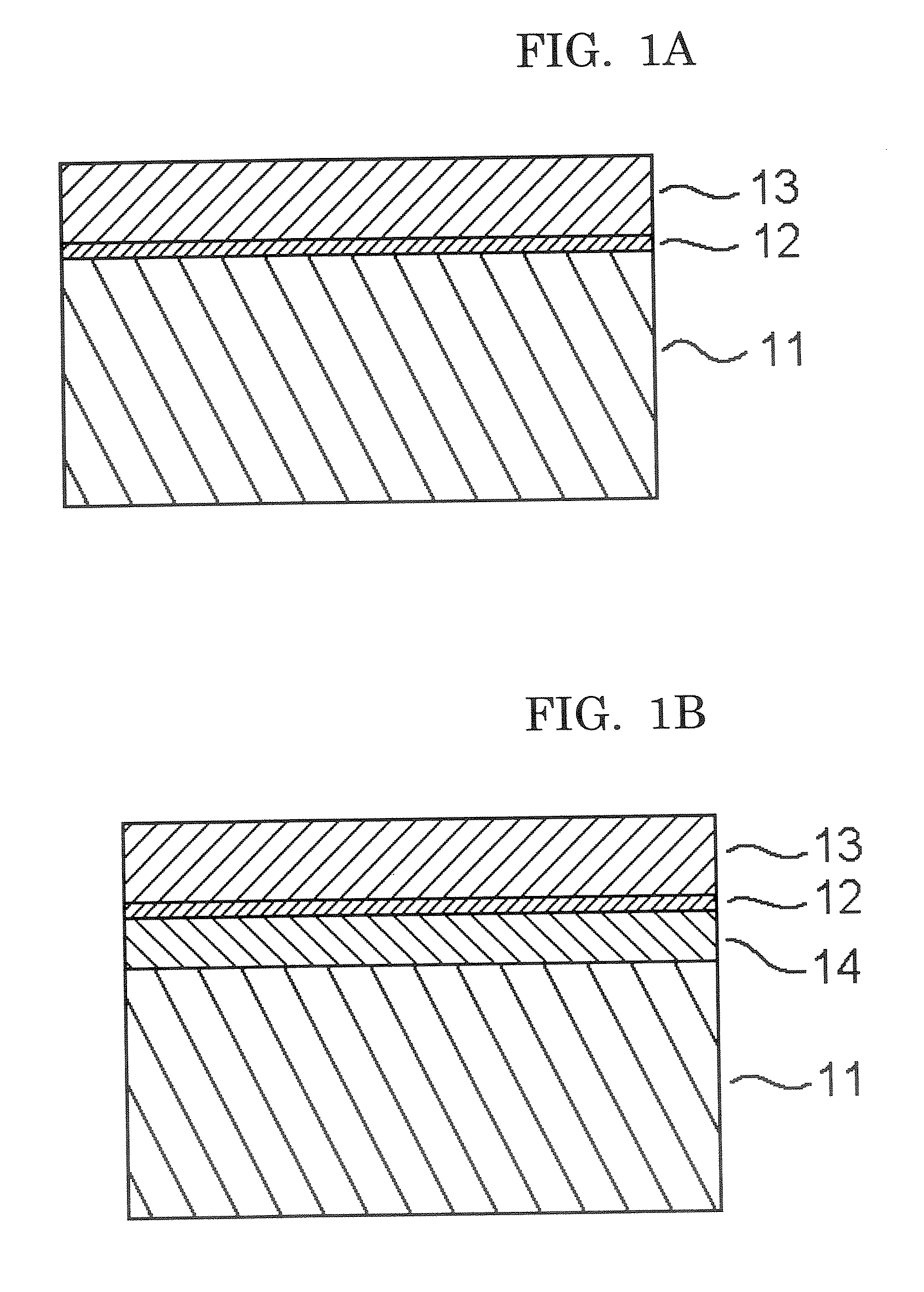
[0244]FIG. 15 A shows a configuration where a charge generating layer 12 that contains a charge generating substance and an optional binder resin and a charge transport layer 13 that contains a charge transport substance and a binder resin are laminated in this order on a support 11. Slight and shallow flaws have generated on the surface 13 of the electrophotographic photoconductor in the circumferential direction through 1000 or more sheets of imaging. The flaws are mainly caused by contact with a cleaning blade or cleaning brush; the ten-point average surface roughness (Rz) is no more than 0.1 μm by use of the surface roughness meter in accordance with JIS B0601-1994.

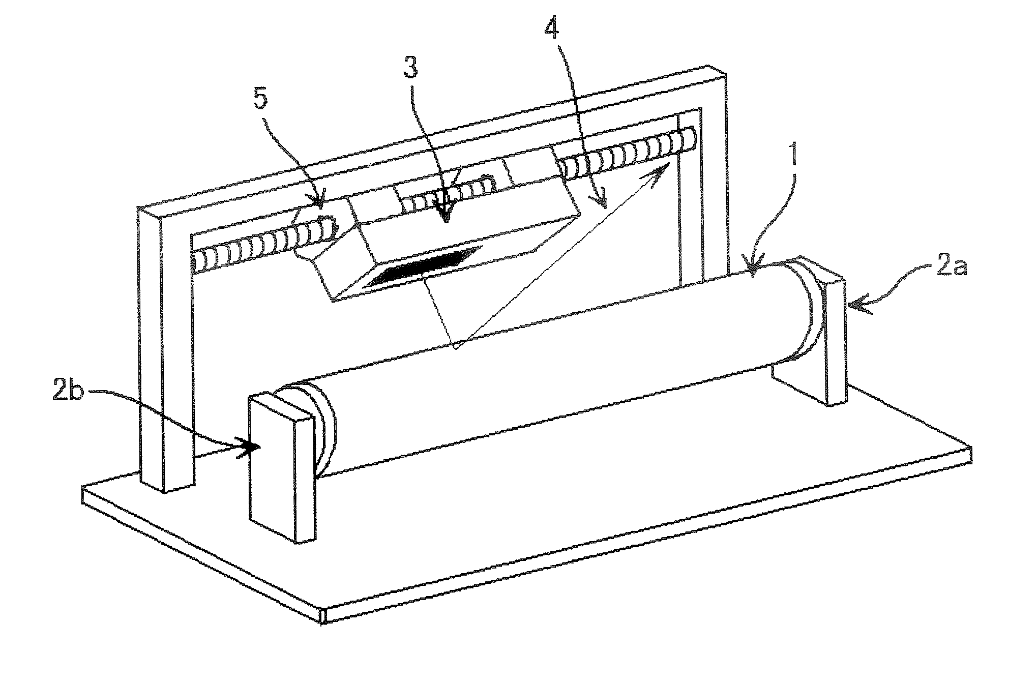
[0245]FIG. 16A is a conceptual view that shows a principal to irradiate UV rays with a wavelength of 200 to 420 nm onto the surface of the electrophotographic photoconductor shown in FIG. 15A and to measure a fluctuation of fluorescence emitted by the electrophotographic photoconductor. Slight and shallow flaws have ...

second embodiment

[0247]FIG. 15 B shows a configuration where an undercoat layer 14 is formed on a support 11, and a charge generating layer 12 that contains a charge generating substance and an optional binder resin and a charge transport layer 13 that contains mainly a charge transport substance and a binder resin are laminated in this order on the undercoat layer. Slight and shallow flaws have generated on the surface of the charge transport layer 13 in the circumferential direction of the electrophotographic photoconductor through 1000 or more sheets of imaging. The flaws are mainly caused by contact with a cleaning blade or cleaning brush; the ten-point average surface roughness (Rz) is no more than 0.1 μm by use of the surface roughness meter in accordance with JIS B0601-1994.

[0248]FIG. 16B is a conceptual view that shows a principal to irradiate UV rays with a wavelength of 200 to 420 nm onto the surface of the electrophotographic photoconductor shown in FIG. 15B and to measure a fluctuation ...

third embodiment

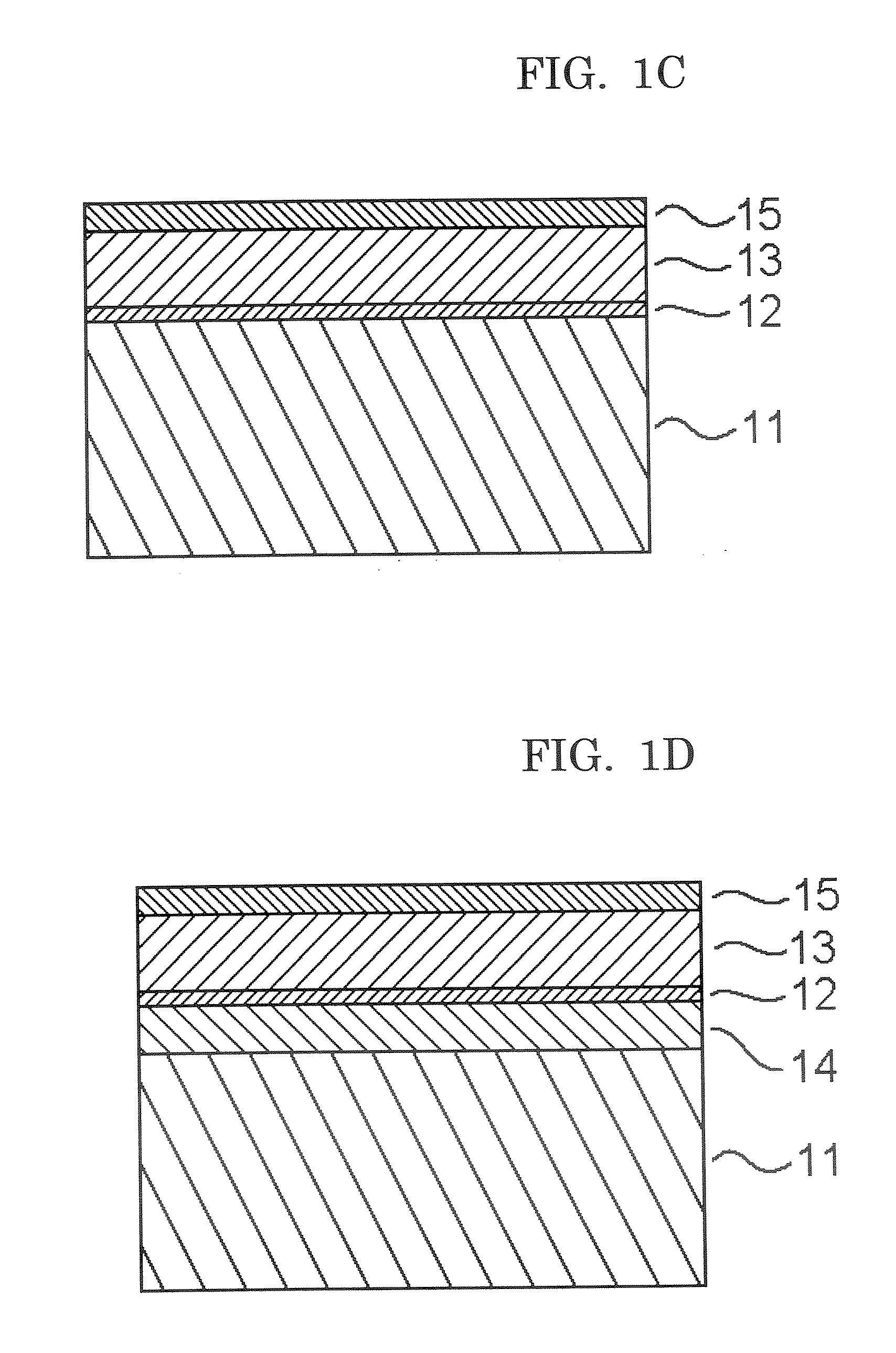
[0250]FIG. 15 C shows a configuration where a charge generating layer 12 that contains a charge generating substance and an optional binder resin, a charge transport layer 13 that contains a charge transport substance and a binder resin, and a protective layer 15 are laminated in this order. In the electrophotographic photoconductor, slight and shallow flaws have generated on the surface of the protective layer 15 in the circumferential direction of the electrophotographic photoconductor through 1000 or more sheets of imaging. The flaws are mainly caused by contact with a cleaning blade or cleaning brush; the ten-point average surface roughness (Rz) is no more than 0.1 μn by use of the surface roughness meter in accordance with JIS B0601-1994.

[0251]FIG. 16C is a conceptual view that shows a principal to irradiate UV rays with a wavelength of 200 to 420 nm onto the surface of the electrophotographic photoconductor shown in FIG. 15C and to measure a fluctuation of fluorescence emitte...


PUM


Abstract

A method for evaluating an electrophotographic photoconductor in terms of filming occurrence is provided that comprises irradiating UV rays having a wavelength of 200 nm to 420 nm onto the electrophotographic photoconductor and measuring fluorescence emitted from the electrophotographic photoconductor.

Description

BACKGROUND OF THE INVENTION [0001] 1. Field of the Invention [0002] The present invention relates to methods for evaluating filming occurrence on electrophotographic photoconductors (hereinafter sometimes referred to as “photoconductor”, “latent electrostatic bearing member”, or “image bearing member”), devices for evaluating electrophotographic photoconductors, and methods for reusing electrophotographic photoconductors. The “evaluation of filming occurrence” in the present invention encompasses the evaluations with respect to existence or nonexistence of filming, degree of filming, and quantification of filming. [0003] 2. Description of the Related Art [0004] In electrophotographic image forming apparatuses, such problems as so-called “filming phenomena” are likely to occur, where paper powders, toner components, fine carrier particles etc. deposit or adhere on surfaces of electrophotographic photoconductors when images are formed repeatedly. [0005] Here, the term “filming phenome...

Claims


Application Information

Patent Timeline
Patent Type & Authority Applications(United States)
IPC IPC(8): G03G15/00
CPCG03G15/5037
Inventor YAMAZAKI, JUNICHINAKATSUGAWA, SHIGEMITSUMAEDA, KENJI
Owner RICOH KK
Why Eureka
Try Eureka