

Multilayer printed circuit board for high-speed differential signal, communication apparatus, and data storage apparatus
a printed circuit board and differential signal technology, applied in the field of printed circuit boards, can solve the problems of reflection noise, distortion, distortion of waveform, etc., and achieve the effect of reducing the coupling degree between differential signal transmission lines, reducing the reflection of backward crosstalk, and reducing the jitter accordingly
- Summary
- Abstract
- Description
- Claims
- Application Information
AI Technical Summary
Benefits of technology
Problems solved by technology
Method used
Image

Examples
first embodiment
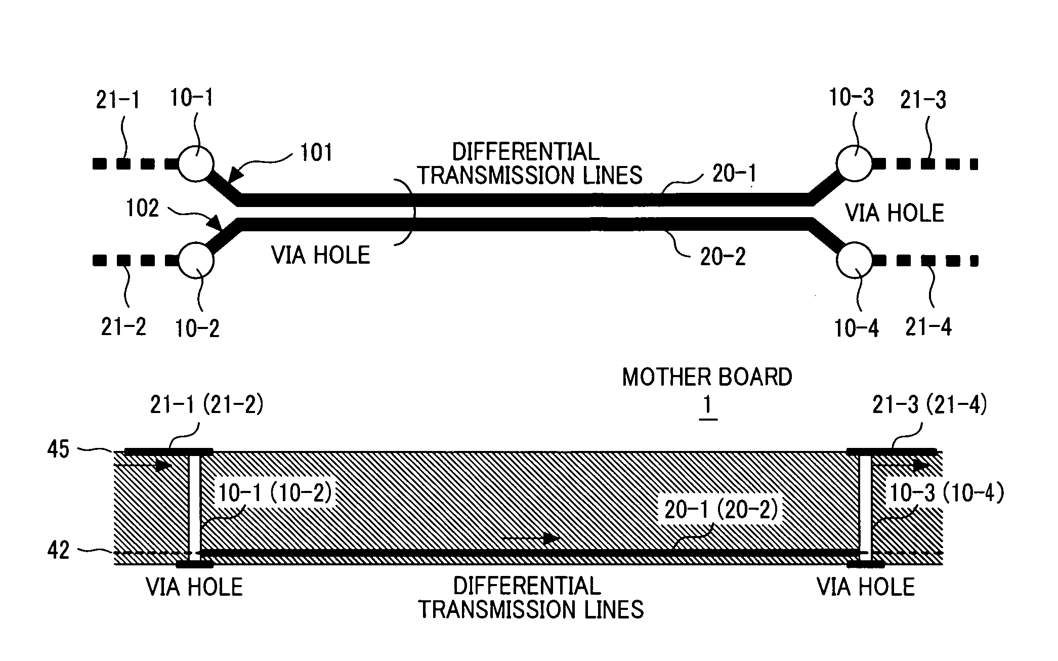
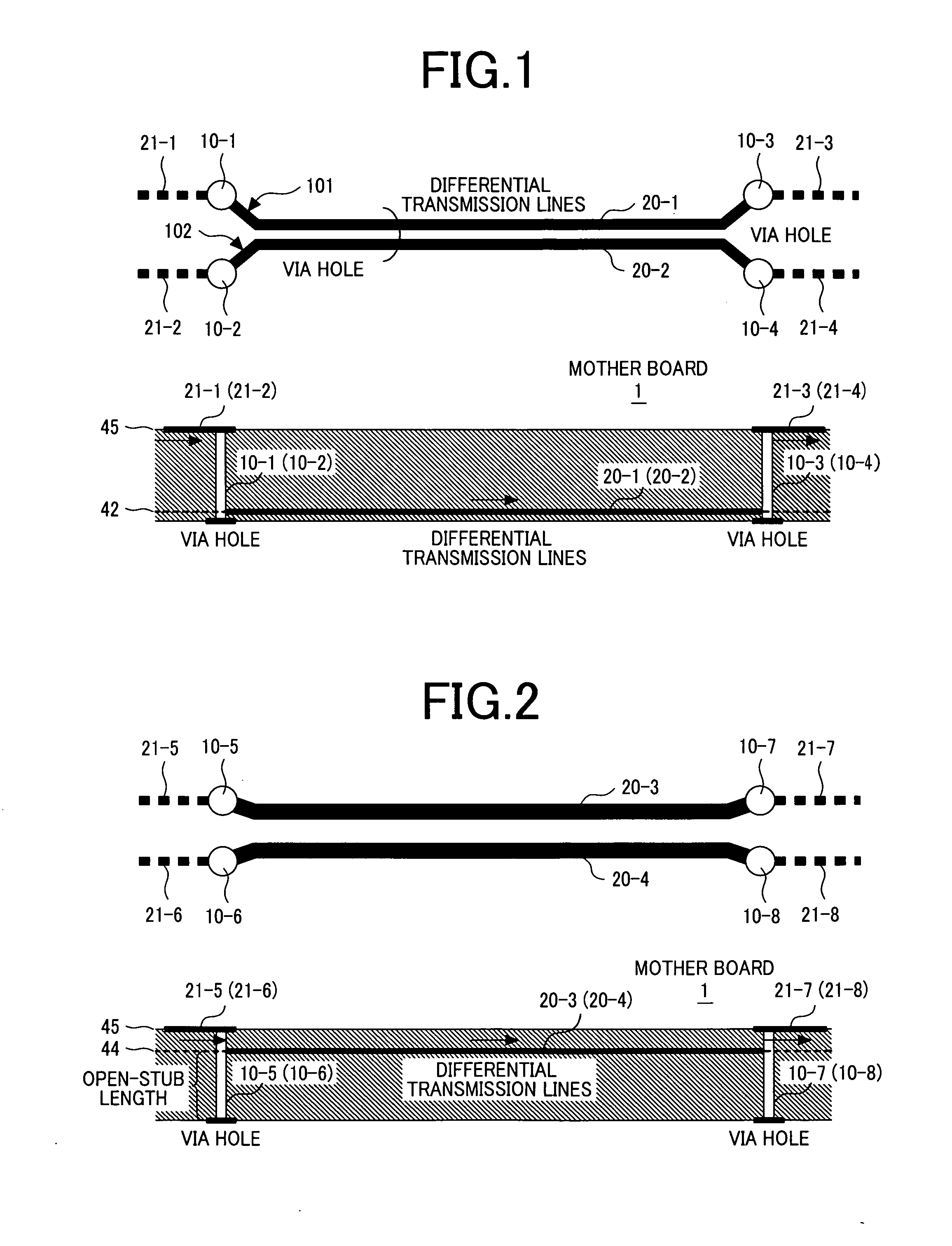
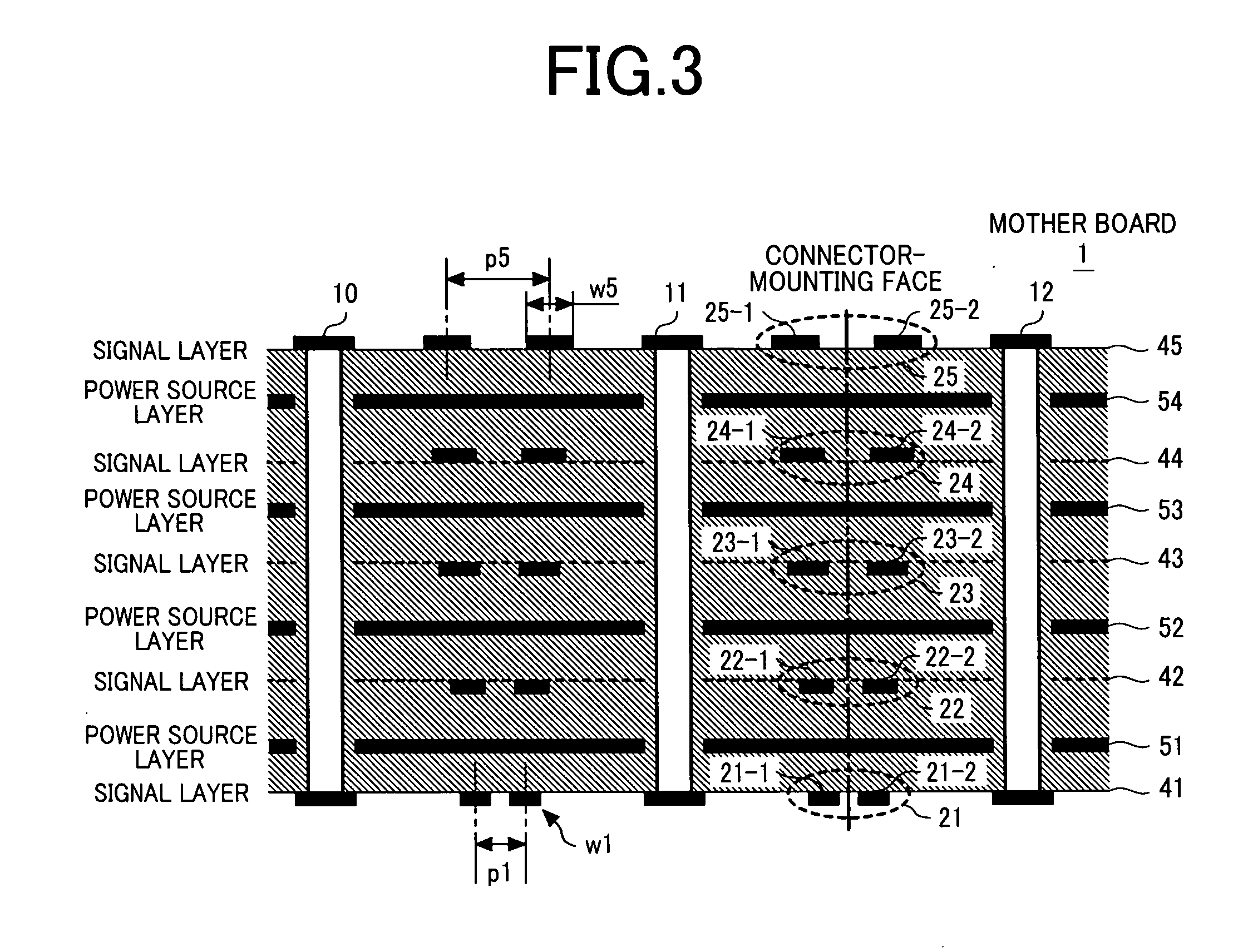
[0039] The first embodiment will be described using FIGS. 1 to 7. FIG. 1 is a plan view and a cross sectional view of a printed circuit board having via holes with a short open-stub length. FIG. 2 is a plan view and a cross sectional view of a printed circuit board having via holes with a long open-stub length. FIG. 3 is a sectional side view of a printed circuit board having layers, each having different line-spacing between transmission lines. FIG. 4 is a bird's eye perspective view of a via hole with a long open-stub length. FIG. 5 is a diagram for explaining pairs of differential transmission lines, each pair having a different degree of coupling. FIG. 6 is a diagram for explaining a signal propagation characteristic with an open-stub length as a parameter. FIG. 7 is a diagram for explaining signal jitter caused by via holes with open-stub lengths and differential transmission lines each having different line-spacing.
[0040] In FIGS. 1 and 2, a multilayer mother board 1 includes...
second embodiment
[0070] The second embodiment will be described using FIGS. 8 to 11. In the second embodiment, the structure of the differential signal transmission lines in the first embodiment is applied to a backplane bus. FIG. 8 is a plan view of plural printed circuit boards configuring a backplane bus. FIGS. 9 and 10 are diagrams for explaining wiring structures of connector portions. FIG. 11 is a bird's eye view of plural printed circuit boards configuring a backplane bus.
[0071] As being apparent with reference to FIG. 11, connectors 70-1 to 70-8 are mounted on a mother board 1 in FIG. 8. Daughter boards can be inserted and mounted to the connectors 70-1 to 70-8. In FIG. 8, the daughter boards 60-1, 60-4, 60-5, and 60-8 are inserted to the connectors 70-1, 70-4, 70-5, and 70-8, respectively. FIG. 8 illustrates eight connectors whereas FIG. 11 illustrates connectors of more than eight. However, the number is not essential so that the connectors are represented by 70-n in FIG. 11. On each daug...
third embodiment
[0081] The third embodiment will be described using FIG. 12. FIG. 12 is a cross sectional view of a multilayer printed circuit board.
[0082] On the mother board 1 shown in FIG. 3, the striplines of the inner layers 42 to 44 are composed of two single-ended transmission lines 23-1 and 23-2 having an extremely low degree of coupling, that is, wide line-spacing, and strongly-coupled microstriplines 21-1 and 21-2 are arranged on the outer layers 41 and 45. All the transmission lines have the same differential impedance.
[0083] The waveform 91 in FIG. 7 represents the jitter in a system in which the wiring of the microstrip structure is connected to via holes with no open-stub lengths. Here again, it can be found that the jitter of the waveform 91 is decreased as the degree of coupling of the transmission lines becomes higher, that is, in the order of the wiring type D to A. The waveform 91 is obtained from the wiring of the wiring layers 45 and 41 in FIG. 3. Since these layers are surfa...
PUM
 Abstract
Description
Claims
Application Information