This helps you quickly interpret patents by identifying the three key elements:
Problems solved by technology
Method used
Benefits of technology
Benefits of technology
[0002] A light-emitting element having a light-emitting layer has been used for a display recently. Such a display using a light-emitting element has advantageous effects such as a wide viewing angle, a high-response speed and low power consumption, as compared with a display having a liquid-crystal layer, and thus, has been developed actively.
[0003] Light-emitting elements have a problem that their light-extraction efficiency is low due to scattered light or reflected light inside the light-emitting elements. The light-extraction efficiency needs to be enhanced.
[0004] In order to enhance the light-extraction efficiency, there is proposed a structure in which a transparent electrode used for an electrode of a light-emitting element has a different thickness according to emission colors (Reference 1: Japanese Patent Laid-Open No. 2003-142277). DISCLOSURE OF INVENTION
[0005] It is an object of the present invention to enhance the light-extraction efficiency of a light-emitting element by a method different from that of Reference 1.
[0006] In order to achieve the object, a thickness of a layer constituting a part of a light-emitting element is made different depending on each emission color, which is one feature of the present invention.
[0007] One mode of the present invention is a light-emitting device comprising a plurality of light-emitting elements. The plurality of light-emitting elements each include a first electrode and a second electrode; and a first layer, a second layer and a third layer which are sequentially formed between the first electrode and the second electrode, wherein the first layer serves as a layer generating holes, the second layer serves as a layer including a light-emitting layer for each emission color, and the third layer serves as a layer generating electrons, and the thickness of the first layer is different depending on each layer including a light-emitting layer.
Problems solved by technology
Light-emitting elements have a problem that their light-extraction efficiency is low due to scattered light or reflected light inside the light-emitting elements.
Method used
Image
Click on the blue label to locate the original text in one second.
Reading with bidirectional positioning of images and text.
Examples
embodiment mode 1
[0043] Embodiment Mode 1 describes a structure of a light-emitting element.
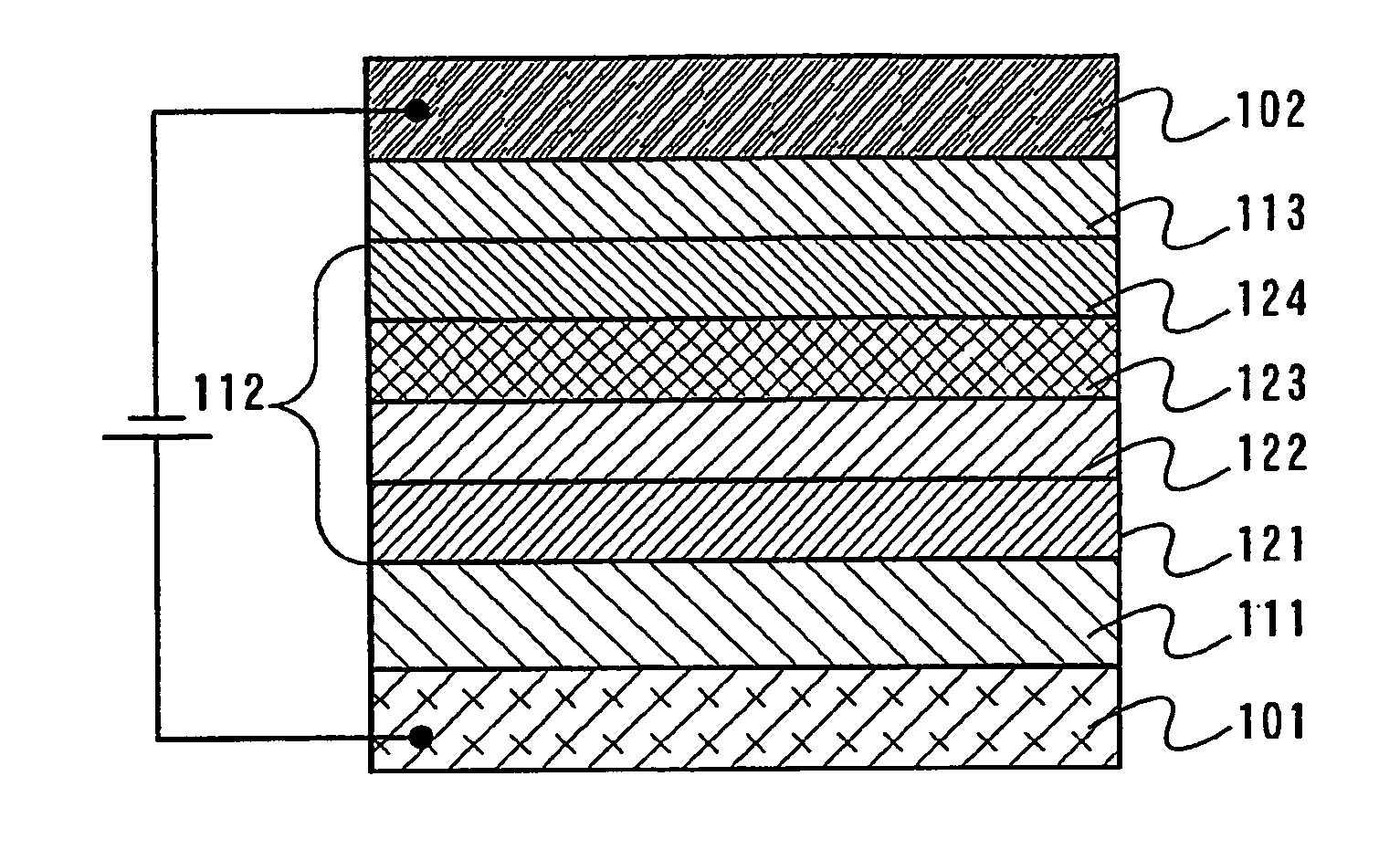
[0044] As shown in FIG. 1, a light-emitting element of the present invention includes a first electrode 101 and a second electrode 102 that are opposed to each other, and a first layer 111, a second layer 112 and a third layer 113 are stacked in this order over the first electrode 101. In such a light-emitting element, holes are injected into the second layer 112 from the first layer 111 and electrons are injected into the second layer 112 from the third layer 113, when a voltage is applied to the light-emitting element such that a potential of the first electrode 101 are higher than that of the second electrode 102. The holes and electrons are recombined in the second layer 112 to excite a light-emitting substance. The excited light-emitting substance emits light when returning to the ground state.
[0045] It is one feature of such light-emitting elements that the thickness of at least one of the layers exce...
embodiment mode 2
[0058] Embodiment Mode 2 describes a structure of a light-emitting element which is different from that of Embodiment Mode 1.
[0059] As shown in FIG. 15, a light-emitting element shown in this embodiment mode includes the first electrode 101 and the second electrode 102 that are opposed to each other, and the first layer 111, the second layer 112, the third layer 113 and a fourth layer 128 that are sequentially stacked over the first electrode 101. One feature of the light-emitting element is to have the fourth layer 128. The fourth layer 128 can be formed with the same material as that of the first layer 111. Other structures are the same as those of Embodiment Mode 1 and thus, the description thereof is omitted.
[0060] When the fourth layer 128 is provided, damages to underlayers in forming the second electrode 102 can be reduced.
[0061] The thickness of the fourth layer 128 is made different depending qn each light-emitting element emitting each emission color. Consequently, the ...
embodiment mode 3
[0065] Embodiment Mode 3 describes a structure in which the thickness of any of layers is made different in a light-emitting device including a color filter.
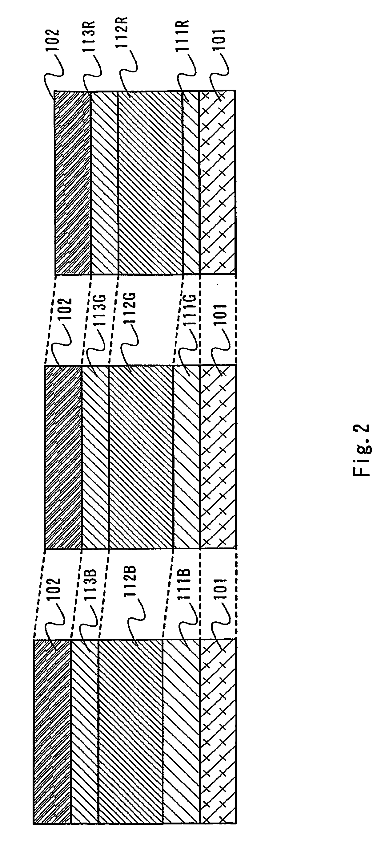
[0066] As shown in FIG. 16, color filters 115R, 115G and 115B are provided in regions that are to exhibit red (R), green (G) and blue (B) that are different in optical characteristics, respectively. The color filters can be formed using a known material by a screen printing method, a droplet discharging method or the like. FIG. 16 shows the case where the color filters 105R, 105G and 105B are provided on the second electrode side 102 (on the emission side), and in this case, the second electrode 102 needs to be light-transmitting.
[0067] The structure of the light-emitting element is as follows: the first layers H1R, H1G and H1B, the second layers 112R, 112G, and 112B, the third layers 113R, 113G and 113B, and the second electrode 102 are formed sequentially over the first electrode 101. Since each color is generated by the col...
PUM
Abstract
Light-emitting elements have a problem that their light-extraction efficiency is low due to scattered light or reflected light inside the light-emitting elements. The light-extraction efficiency of the light-emitting elements needs to be enhanced by a new method. According to the present invention, a light-emitting element includes a first layer generating holes, a second layer including a light-emitting layer for each emission color and a third layer generating electrons between an anode and a cathode, and the thickness of the first layer is different depending on each layer including the light-emitting layer for each emission color. A layer in which an organic compound and a metaloxide are mixed is used as the first layer, and thus, the driving voltage is not increased even when the thickness is increased, which is preferable.
Description
TECHNICAL FIELD [0001] The present invention relates to a light-emitting element having a light-emitting layer, a light-emitting device having the light-emitting element, and a manufacturing method thereof BACKGROUND ART [0002] A light-emitting element having a light-emitting layer has been used for a display recently. Such a display using a light-emitting element has advantageous effects such as a wide viewing angle, a high-response speed and low power consumption, as compared with a display having a liquid-crystal layer, and thus, has been developed actively. [0003] Light-emitting elements have a problem that their light-extraction efficiency is low due to scattered light or reflected light inside the light-emitting elements. The light-extraction efficiency needs to be enhanced. [0004] In order to enhance the light-extraction efficiency, there is proposed a structure in which a transparent electrode used for an electrode of a light-emitting element has a different thickness accord...
Claims
Application Information
Patent Timeline
Application Date:The date an application was filed.
Publication Date:The date a patent or application was officially published.
First Publication Date:The earliest publication date of a patent with the same application number.
Issue Date:Publication date of the patent grant document.
PCT Entry Date:The Entry date of PCT National Phase.
Estimated Expiry Date:The statutory expiry date of a patent right according to the Patent Law, and it is the longest term of protection that the patent right can achieve without the termination of the patent right due to other reasons(Term extension factor has been taken into account ).
Invalid Date:Actual expiry date is based on effective date or publication date of legal transaction data of invalid patent.

