Liquid Crystal Display Device with a Built-in Touch Screen and Method for Manufacturing the Same

Active Publication Date: 2012-03-22
LG DISPLAY CO LTD
View PDF2 Cites 39 Cited by
  • Summary
  • Abstract
  • Description
  • Claims
  • Application Information

AI Technical Summary

Benefits of technology

[0035]An aspect of the present invention is to provide an LCD device with a built-in touch screen, which enhances driving efficiency by using a lower substrate of low-temperature poly silicon (LTPS), and a method for manufacturing the same.
[0036]Another aspect of the present invention is to provide an LCD device with a built-in touch screen, which reduces a manufacturing cost by reducing the number of masks for a process of forming a lower substrate, and a method for manufacturing the same.
[0037]Anot

Problems solved by technology

Accordingly, the process of forming the common electrode 75 is separately carried out from the process of forming the conductive line 76, whereby the manufacturing cost is increased and the yield is deteriorated due to the complicated manufacturing process.
Amorphous silicon (a-Si) TFT

Method used


Image

  • Liquid Crystal Display Device with a Built-in Touch Screen and Method for Manufacturing the Same
  • Liquid Crystal Display Device with a Built-in Touch Screen and Method for Manufacturing the Same
  • Liquid Crystal Display Device with a Built-in Touch Screen and Method for Manufacturing the Same

Examples


Example

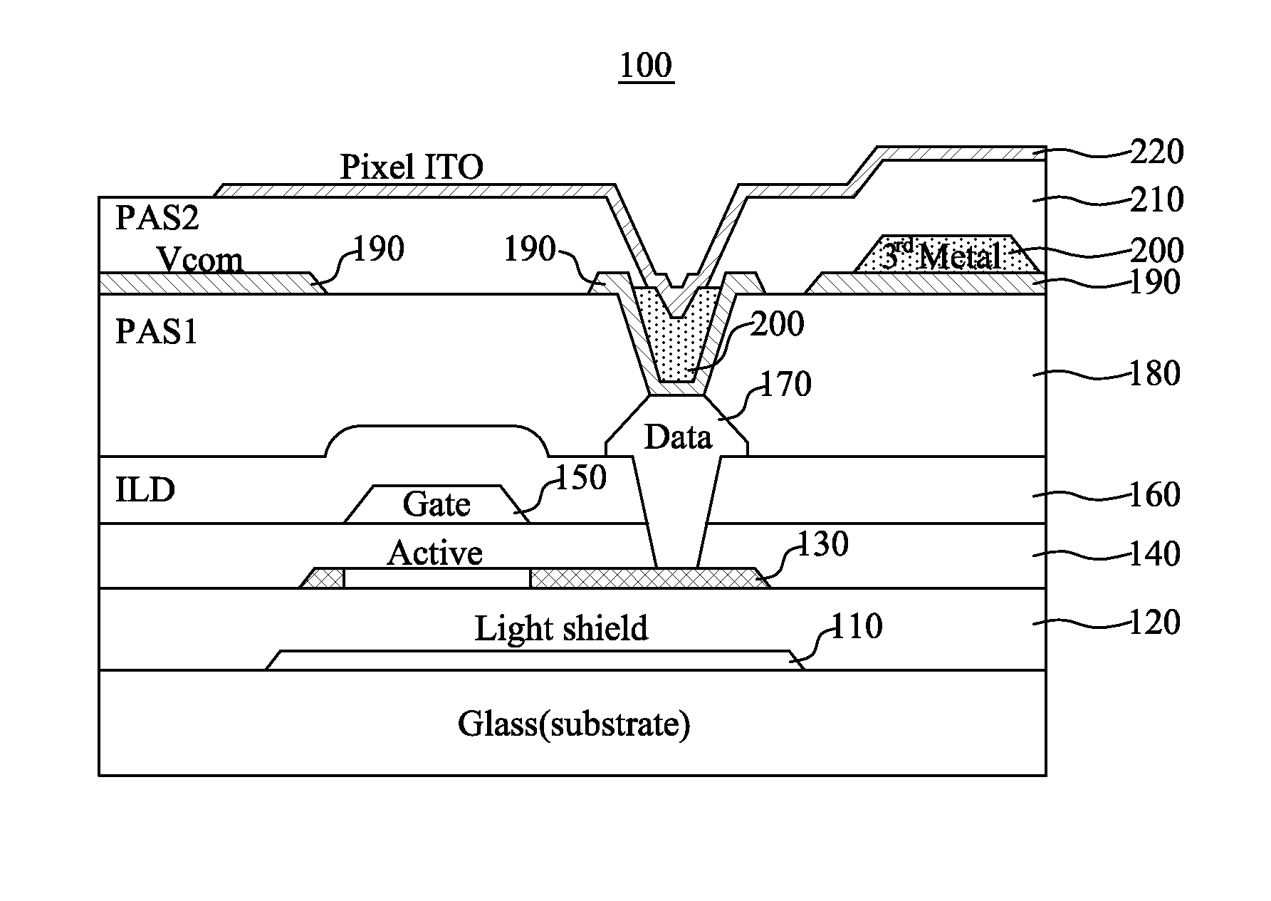
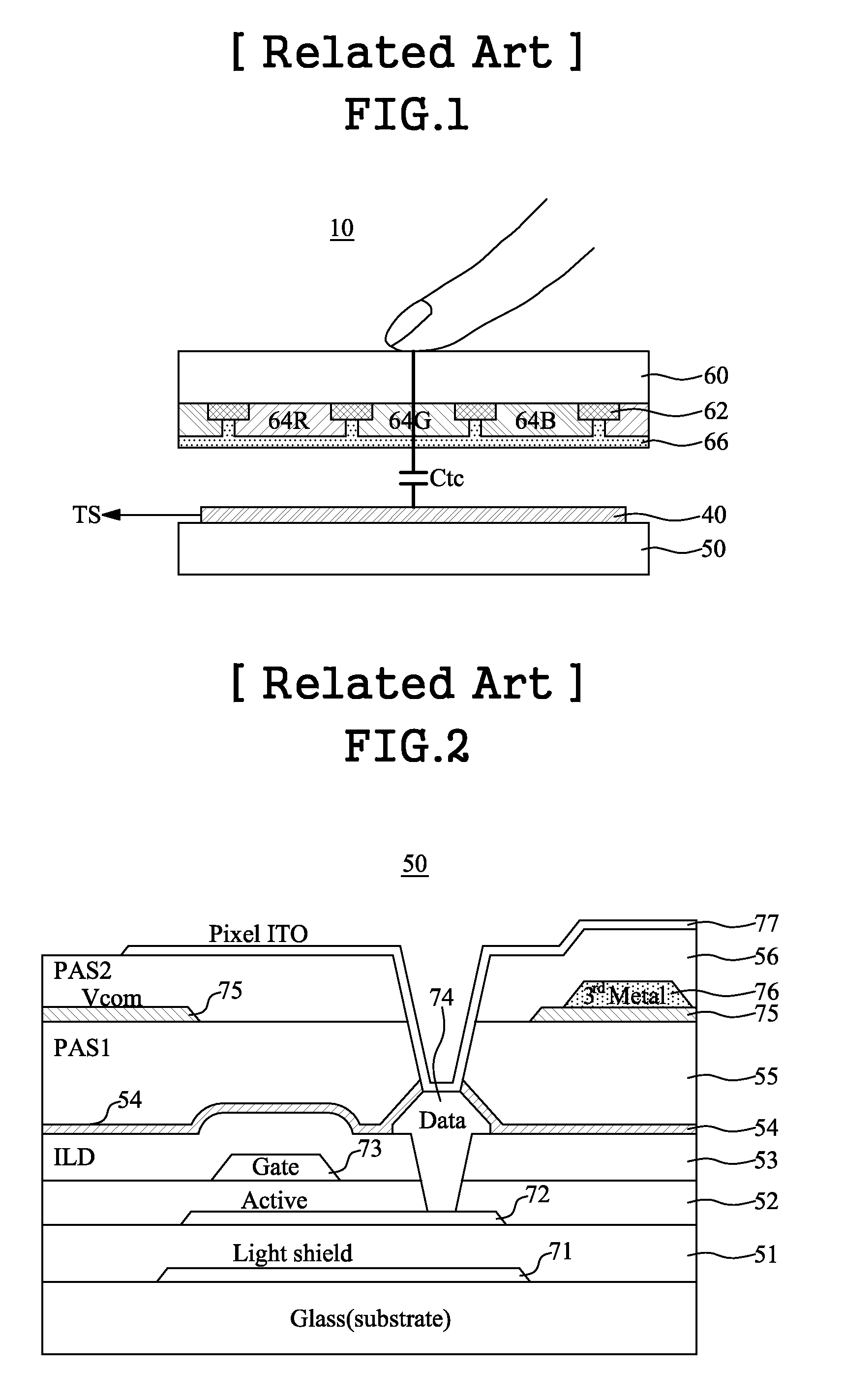
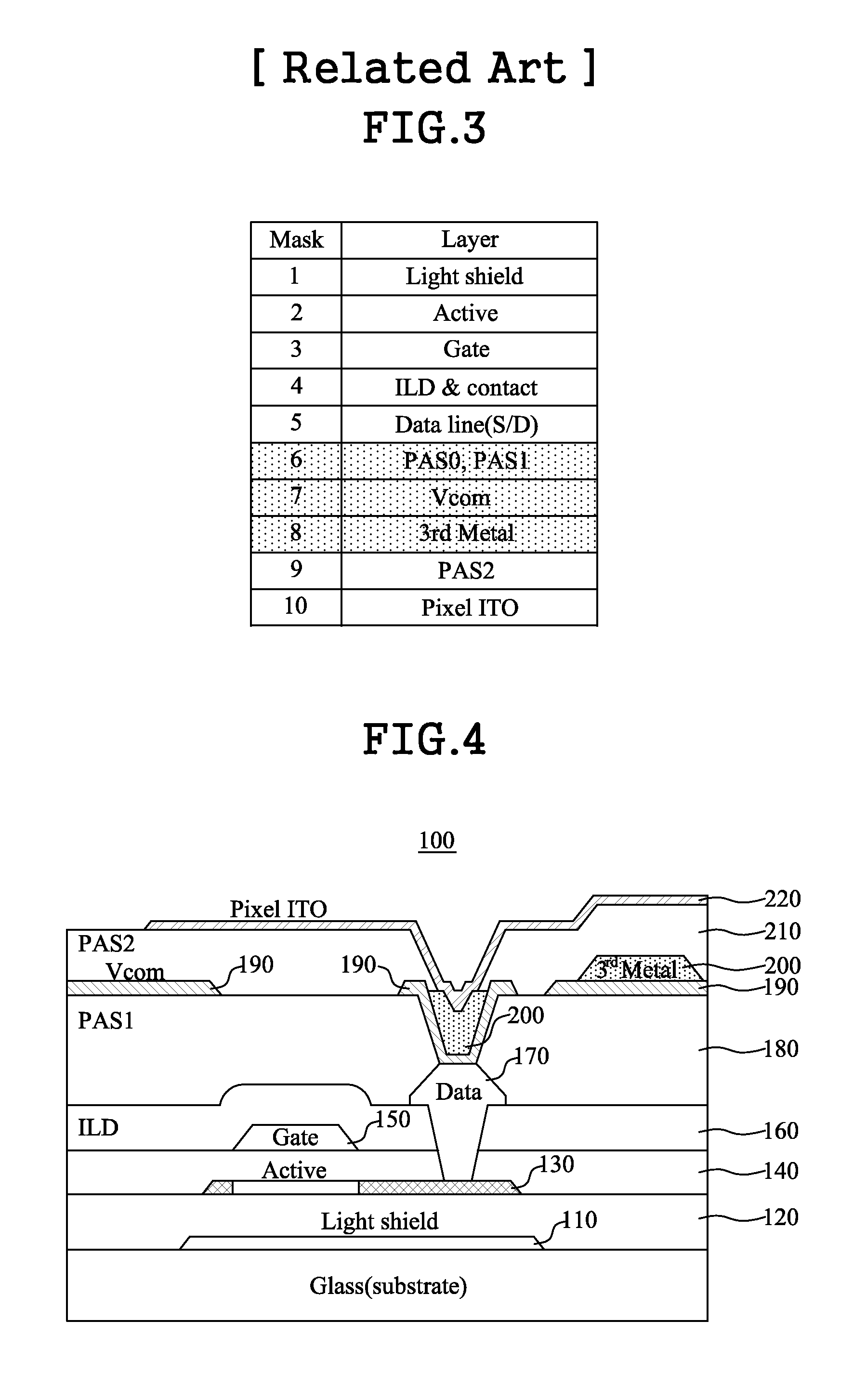
[0054]Reference will now be made in detail to the exemplary embodiments of the present invention, examples of which are illustrated in the accompanying drawings. Wherever possible, the same reference numbers will be used throughout the drawings to refer to the same or like parts.

[0055]Hereinafter, an LCD device with a built-in touch screen according to the present invention and a method for manufacturing the same will be described with reference to the accompanying drawings.

[0056]For the following description of the embodiments of the present invention, if a first structure (for example, electrode, line, layer, contact, and etc.) is described as being formed “on” or “under” a second structure, the first and second structures may come in contact with each other, or there may be a third structure interposed between the first and second structures.

[0057]Depending on an alignment mode of the liquid crystal layer, an LCD device may be classified into Twisted-Nematic (TN) mode, Vertical-A...


PUM


Abstract

A liquid crystal display device with a built-in touch screen comprising a substrate having a pixel region, a thin film transistor formed at the pixel region, the thin film transistor including at least an active layer, a gate electrode, an insulating layer, and a data electrode, a first passivation layer formed on the thin film transistor, a first contact hole formed through a portion of the first passivation layer to expose the data electrode, a common electrode formed on at least one portion of the first passivation layer including inside the first contact hole, the common electrode operable to sense touch, a conductive line formed on at least one portion of the first passivation layer including inside the first contact hole, a second passivation layer formed on the common electrode and the conductive line, a second contact hole formed through a portion of the second passivation layer to expose the conductive line corresponding to the data electrode, and a pixel electrode electrically connected with the conductive line, the pixel electrode formed on the second passivation layer and inside the second contact hole, wherein the data electrode and the pixel electrode are electrically connected via the common electrode and the conductive line.

Description

CROSS REFERENCE TO RELATED APPLICATIONS[0001]This application claims the benefit of the Korean Patent Application No. 10-2010-0092368 filed on Sep. 20, 2010, which is hereby incorporated by reference as if fully set forth herein.BACKGROUND OF THE INVENTION[0002]1. Field of the Invention[0003]The present invention relates to a flat panel display device, and more particularly, a liquid crystal display device with a built-in touch screen, which enhances driving performance, and reduces manufacturing costs by a simplified manufacturing process, and a method for manufacturing the same.[0004]2. Discussion of the Related Art[0005]Recent developments in various mobile electronic equipment such as mobile terminal and notebook computer has increased the demand for an applicable flat panel display device.[0006]The flat panel display device may include a liquid crystal display device (LCD), a plasma display panel (PDP), a field emission display device (FED), a light-emitting diode display devic...

Claims


Application Information

Patent Timeline
IPC IPC(8): G02F1/136H01L33/36
CPCG02F1/13338G02F1/136227G02F2001/13629G06F3/044G06F3/0412G06F2203/04103G02F2001/136295G06F3/0443G02F1/13629G02F1/136295
Inventor OH, KUM MILEE, HAN SEOK
Owner LG DISPLAY CO LTD
Why Eureka
Try Eureka