Gallium-containing light-emitting semiconductor device and method of fabrication

US20050205886A1Inactive Publication Date: 2005-09-22SANKEN ELECTRIC CO LTD

Image

  • Gallium-containing light-emitting semiconductor device and method of fabrication
  • Gallium-containing light-emitting semiconductor device and method of fabrication
  • Gallium-containing light-emitting semiconductor device and method of fabrication

Examples


embodiment

of FIG. 10

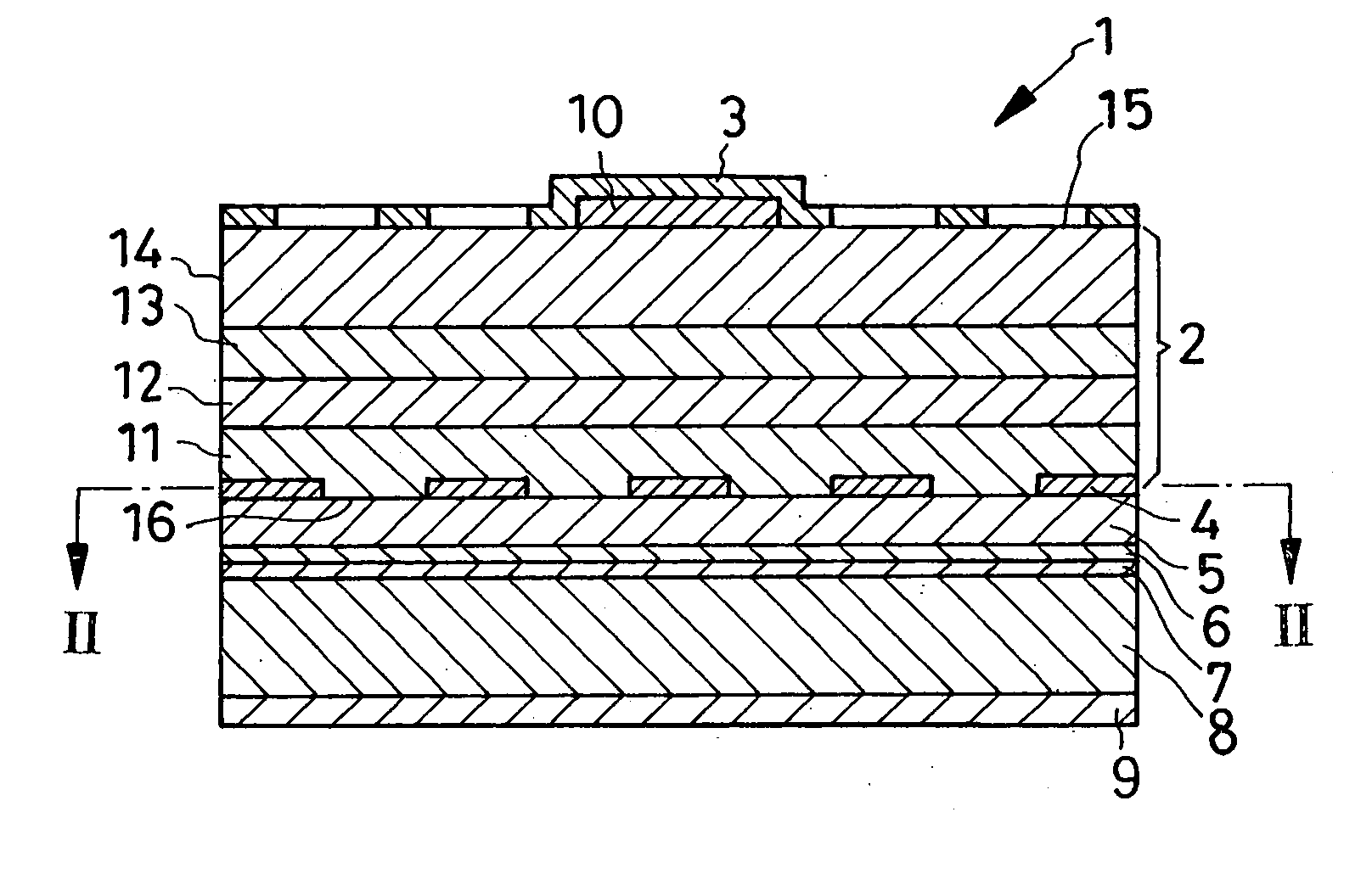
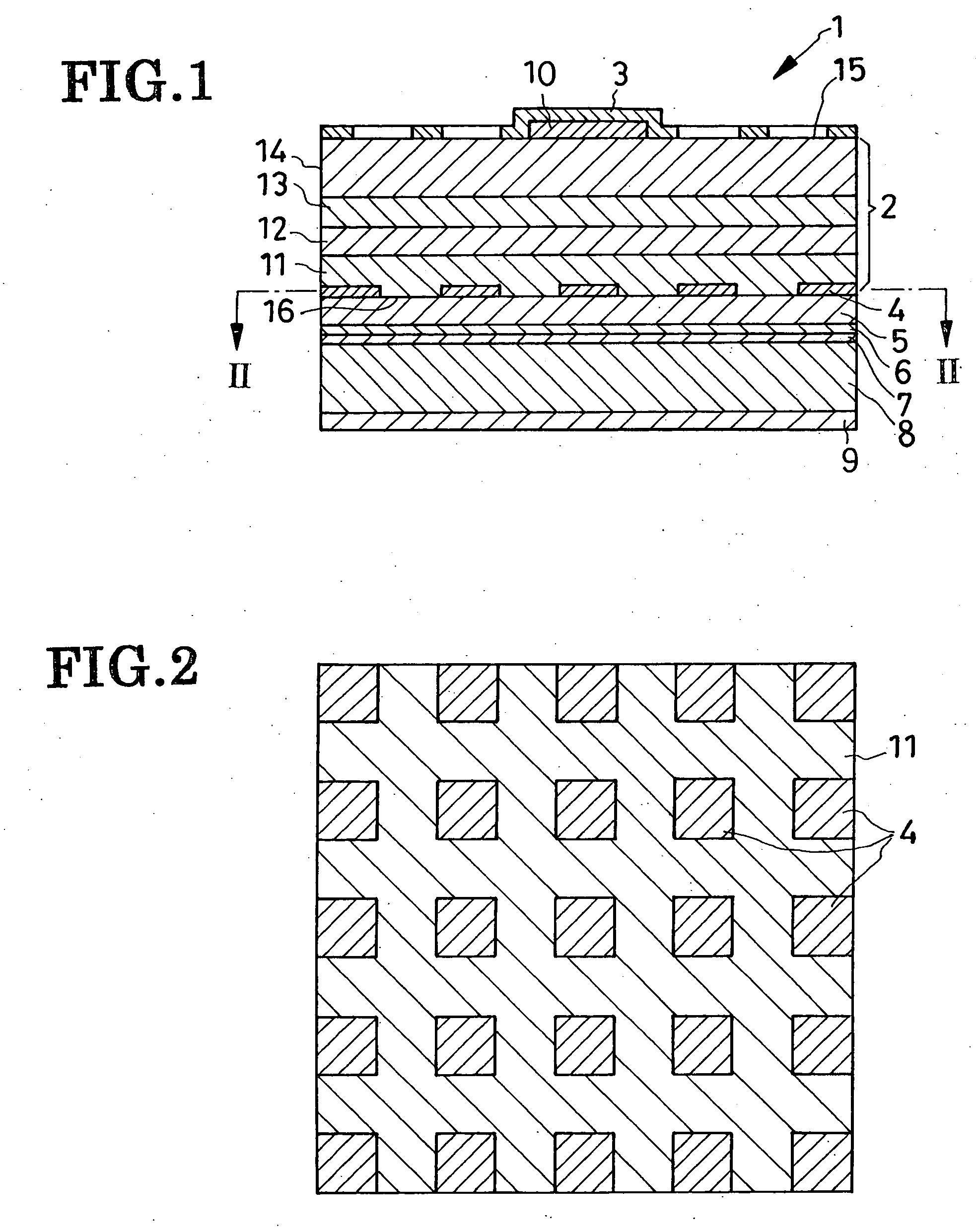
[0082] Another preferred form of LED 1a shown in FIG. 1 has an integral ohmic contact region 4a covering the entire bottom surface 16 of the lower cladding 11. A relatively high efficiency is nevertheless obtainable because the total reflectivity of the ohmic contact region 4a and reflective layer 5 is as high as 60 percent. As the ohmic contact region 4a is larger than all the isolated ohmic contact regions 4 of FIGS. 1 and 2 combined, so much is reduced the resistance to forward current flow, with a corresponding diminution of power loss.

[0083] Another feature of the alternative LED 1a resides in a metal-made baseplate 8a which is affixed to the reflective layer 5 under heat and pressure in place of the silicon baseplate 8 of the previous embodiment. No dedicated cathode is provided as the baseplate 8a serves as both mechanical support and cathode.

[0084] The alternative LED 1a is akin to the first disclosed LED 1 in all the other details of construction. The integrated...


PUM


Abstract

An LED comprising a light-generating semiconductor region having an active layer sandwiched between two confining layers of opposite conductivity types. A cathode is arranged centrally on one of the opposite major surfaces of the semiconductor region from which is emitted the light. An array of discrete gold regions are formed via transition metal regions on the other major surface of the semiconductor region at which is exposed one of the confining layers which is of n-type AlGaInP semiconductor material. The gold is thermally diffused into the confining layer via the transition metal regions at a temperature less than the eutectic point of gold and gallium, thereby creating an array of ohmic contact regions of alloyed or intermingled gold and gallium, which are less absorptive of light than their conventional counterparts, to a thickness of 20 to 1000 angstroms. After removing the transition metal regions and gold regions from the surface of the light-generating semiconductor region, a reflective layer of aluminum is formed so as to cover both the ohmic contact regions and the exposed surface portions of the AlGaInP confining layer. An electroconductive base-plate of doped silicon is then bonded to the reflective layer.

Description

CROSS REFERENCE TO RELATED APPLICATIONS [0001] This is a continuation of Application PCT / JP2003 / 014890, filed Nov. 21, 2003, which claims priority to Japanese Patent Application No. 2002-348416 filed Nov. 29, 2002.BACKGROUND OF THE INVENTION [0002] This invention relates to a light-emitting semiconductor device, or light-emitting diode (LED) according to more common parlance, and more particularly to such devices employing gallium-containing compound semiconductors. The invention also concerns a method of making such light-emitting semiconductor devices. [0003] The LED has been known which has a light-generating semiconductor region grown on a substrate of electrically conducting material such as gallium arsenide. Typically, the light-generating semiconductor region has an active layer sandwiched between an n-type cladding or lower confining layer, which overlies the substrate, and a p-type cladding or upper confining layer. An anode is mounted centrally atop the upper confining lay...

Claims


Application Information

Patent Timeline
22 Sep 2005
Publication
US20050205886A1
IPC
H01L21/18; H01L21/22; H01L29/22; H01L33/00; H01L33/20; H01L33/38; H01L33/40
CPC
H01L21/182; H01L21/2215; H01L33/405; H01L33/20; H01L33/387; H01L33/0079; H01L33/0093
Inventors
MUROFUSHI, HITOSHI; TAKEDA, SHIRO